Semiconductor memory having an error correction function

a technology of semiconductor memory and function, which is applied in the field of semiconductor memory having an error correction function, can solve the problems of switch circuit making the switch function ineffective, and it is difficult to write a desired pattern to the parity cell array

Inactive Publication Date: 2007-05-01
SOCIONEXT INC
View PDF4 Cites 8 Cited by
  • Summary
  • Abstract
  • Description
  • Claims
  • Application Information

AI Technical Summary

Benefits of technology

[0010]According to a first aspect of a semiconductor memory of the present invention, regular data inputted / outputted to / from an external data terminal is read / written from / to a regular cell array, and parity data is read / written from / to a parity cell array. Since the parity data is generated by a parity generation circuit, it is difficult to write a desired pattern to the parity cell array. The read data from the regular cell array is corrected by an error correction circuit according to the parity data. In this invention, a switch circuit exchanges the regular data and the parity data with each other to enable write of the regular data to the parity cell array and write of the parity data to the regular cell array. This makes it possible to write desired data to the parity cell array to facilitate conducting a test of the parity cell array. In particular, a leakage test and the like between memory cells can be easily conducted. Since only the storage destinations of the regular data and the parity data are exchanged, it is possible to conduct the test while the parity generation circuit and the error correction circuit are in operation. That is, the test can be conducted while the same circuit operations as normal operations are performed.
[0011]In a preferable example of the first aspect of the semiconductor memory of the present invention, a test control circuit activates a test signal in response to a test command in order to shift a state of the semiconductor memory from a normal operation mode to a test mode. The switch circuit makes a switch function effective in the test mode during which the test signal is active to input / output the regular data to / from the parity cell array and input / output the parity data to / from the regular cell array. On the other hand, the switch circuit makes the switch function ineffective in the normal operation mode during which the test signal is inactive to input / output the regular data to / from the regular cell array and input / output the parity data to / from the parity cell array. Controlling the operation of the switch circuit according to the test command can facilitate and ensure switching of the switch circuit.
[0012]In a preferable example of the first aspect of the semiconductor memory of the present invention, read amplifiers are provided for the regular cell array and the parity cell array, respectively, each of the read amplifiers being provided for each bit of read data in order to amplify an amount of signal of the read data. Write amplifiers are provided for the regular cell array and the parity cell array, respectively, each of the write amplifiers being provided for each bit of write data in order to amplify an amount of signal of the write data. The switch circuit is constituted of a plurality of sub switch circuits corresponding to the bits of the read / write data, respectively. Each of the sub switch circuits has a write selector and a read selector. The write selector outputs the write data to the write amplifier of one of the regular cell array and the parity cell array. The read selector outputs to a data line the read data from the read amplifier of one of the regular cell array and the parity cell array. Constituting the switch circuit of the plural sub switch circuits can facilitate circuit designing and shorten a design period.

Problems solved by technology

Since the parity data is generated by a parity generation circuit, it is difficult to write a desired pattern to the parity cell array.
On the other hand, the switch circuit makes the switch function ineffective in the normal operation mode during which the test signal is inactive to input / output the regular data to / from the regular cell array and input / output the parity data to / from the parity cell array.

Method used


Image

  • Semiconductor memory having an error correction function
  • Semiconductor memory having an error correction function
  • Semiconductor memory having an error correction function

Examples


first embodiment

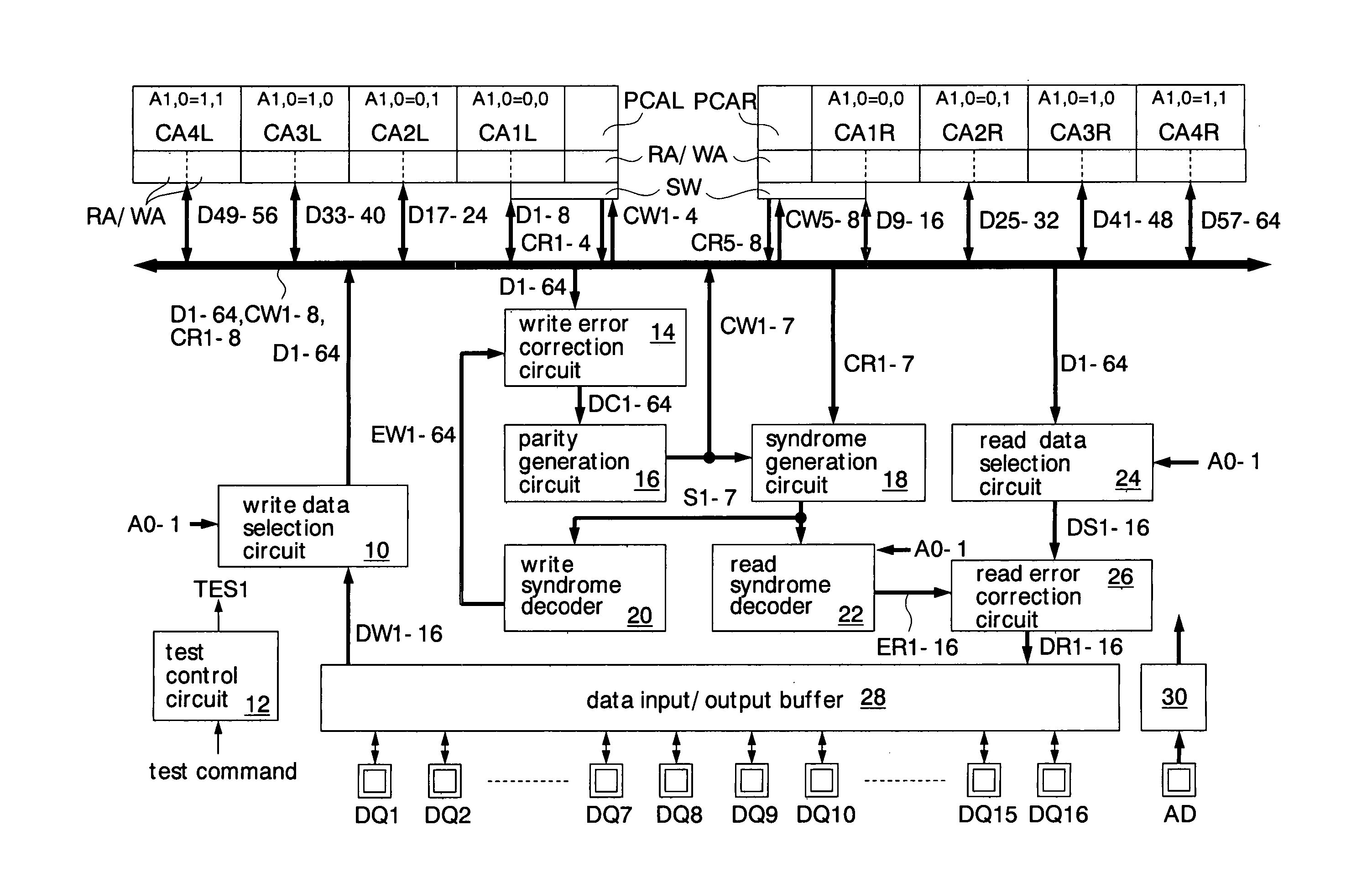
[0053]FIG. 1 shows the semiconductor memory of the present invention. This semiconductor memory is formed as a pseudo SRAM on a silicon substrate by using a CMOS process. The pseudo SRAM has a memory core of a DRAM memory core and an SRAM interface.

[0054]The pseudo SRAM has regular cell arrays CA1 (CA1L, CA1R), CA2 (CA2L, CA2R), CA3 (CA3L, CA3R), CA4 (CA4L, CA4R) storing regular data supplied via external data terminals DQ1–16, parity cell arrays PCA (PCAL, PCAR) storing parity data, read amplifiers RA / write amplifiers WA, switch circuits SW, a write data selection circuit 10, a test control circuit 12, a write error correction circuit 14, a parity generation circuit 16, a syndrome generation circuit 18, a write syndrome decoder 20, a read syndrome decoder 22, a read data selection circuit 24, a read error correction circuit 26, a data input / output buffer 28, and an address buffer 30.

[0055]In addition to those shown in the drawing, the pseudo SRAM has an address decoder, command ter...

second embodiment

[0123]FIG. 14 shows a comparative example of the The same reference codes are used to designate the same elements as the elements in FIG. 9. In this example, each syndrome generation circuit 40A generates syndromes S1–4 (or S5–8) by using read data DR1–8 (or D9–16) and parity read data PR1–4 outputted from a switch circuit 48.

[0124]FIG. 15 shows details of the syndrome generation circuit 40A shown in FIG. 14. The syndrome generation circuit 40A is constituted of four circuit blocks for generating the 4-bit syndrome values S1–4. Each of the blocks has two 3-input exclusive-OR circuits XOR3 and a 2-input exclusive-OR circuit XOR2.

[0125]Parenthesized data out of input data of the exclusive-OR circuits XOR3 represent data actually received (exchange data) in the test mode. For example, the block generating the syndrome value S1 receives data D2–4, D6, D7, P1 in the normal operation mode, and receives data P2–4, D6, D7, D1 in the test mode. Therefore, the syndrome generation circuit 40A...

third embodiment

[0146]Since the inversion of the parity data CW2–3 is not necessary irrespective of the logics of the write data D1–64, the inversion circuit SINV of this embodiment is structured such that terminals receiving inversion control signals (TINV2–3 of the third embodiment) of the sub inversion circuits SINV corresponding to the parity data CW2–3 (CR2–3) are connected to a ground line VSS (dummy sub inversion circuits). Therefore, the dummy inversion circuits always output the parity data CW2–3 (CRI2–3) as they are without inverting them. Terminals receiving the inversion control signals in the other sub inversion circuits SINV receive a common inversion control signal TINV00. Since the operations of the plural sub inversion circuits SINV can be simultaneously controlled with the common inversion control signal TINV00, the inversion control circuit 36 can have a simple structure. Further, a wiring area of a signal line for transmitting the inversion control signal TINV00 can be made smal...


PUM


Abstract

Regular data inputted / outputted to / from external terminals is read / written to / from a regular cell array, and parity data is read / written from / to a parity cell array. Since the parity data is generated by a parity generation circuit, it is difficult to write a desired pattern to the parity cell array. The regular data and the parity data are exchanged with each other by a switch circuit, so that the regular data can be written to the parity cell array and the parity data can be written to the regular cell array. This enables the write of desired data to the parity cell array. A test of the parity data can be easily conducted. In particular, a leakage test or the like between memory cells can be easily conducted.

Description

CROSS-REFERENCE TO RELATED APPLICATIONS[0001]This application is based upon and claims the benefit of priority from Japanese Patent Application Nos. 2004-368016 and 2005-073391, each filed on Dec. 20, 2004 and Mar. 15, 2005, the entire contents of which are incorporated herein by reference.BACKGROUND OF THE INVENTION[0002]1. Field of the Invention[0003]The present invention relates to a semiconductor memory having an error correction function.[0004]2. Description of the Related Art[0005]A semiconductor memory having an error correction function has regular cell arrays storing externally supplied data and parity cell arrays storing parity data of data written to the regular cell arrays. The parity data are generated by a parity generation circuit according to the write data. Data read from the regular cell arrays are error-corrected by an error correction circuit according to the parity data. It is not generally easy to write desired data to the parity cell arrays, which makes a test...

Claims


Application Information

Patent Timeline
Patent Type & Authority Patents(United States)
IPC IPC(8): G11C29/00
CPCG06F11/1032G11C29/24G11C29/50016G11C29/52G11C11/401G11C2029/0409
Inventor KIKUTAKE, AKIRAONISHI, YASUHIROKAWABATA, KUNINORISASAKI, JUNICHIMIYO, TOSHIYA
Owner SOCIONEXT INC
Why Eureka
Try Eureka