Electronic circuit connecting structure, and its connecting method

Inactive Publication Date: 2007-05-08
PANASONIC CORP
View PDF13 Cites 32 Cited by
  • Summary
  • Abstract
  • Description
  • Claims
  • Application Information

AI Technical Summary

Benefits of technology

[0007]The present invention has been made taking these points into consideration, and the object of the invention is to provide an electronic circuit connecting st

Problems solved by technology

However, when the connecting pitch is lessened, there arise the following problems.
If the second connection land of the flexible board is reduced in thickness, the insulating layer on the circuit board in the first example will be hard to effectively prevent the solder from running

Method used


Image

  • Electronic circuit connecting structure, and its connecting method
  • Electronic circuit connecting structure, and its connecting method
  • Electronic circuit connecting structure, and its connecting method

Examples


Example

First Exemplary Embodiment

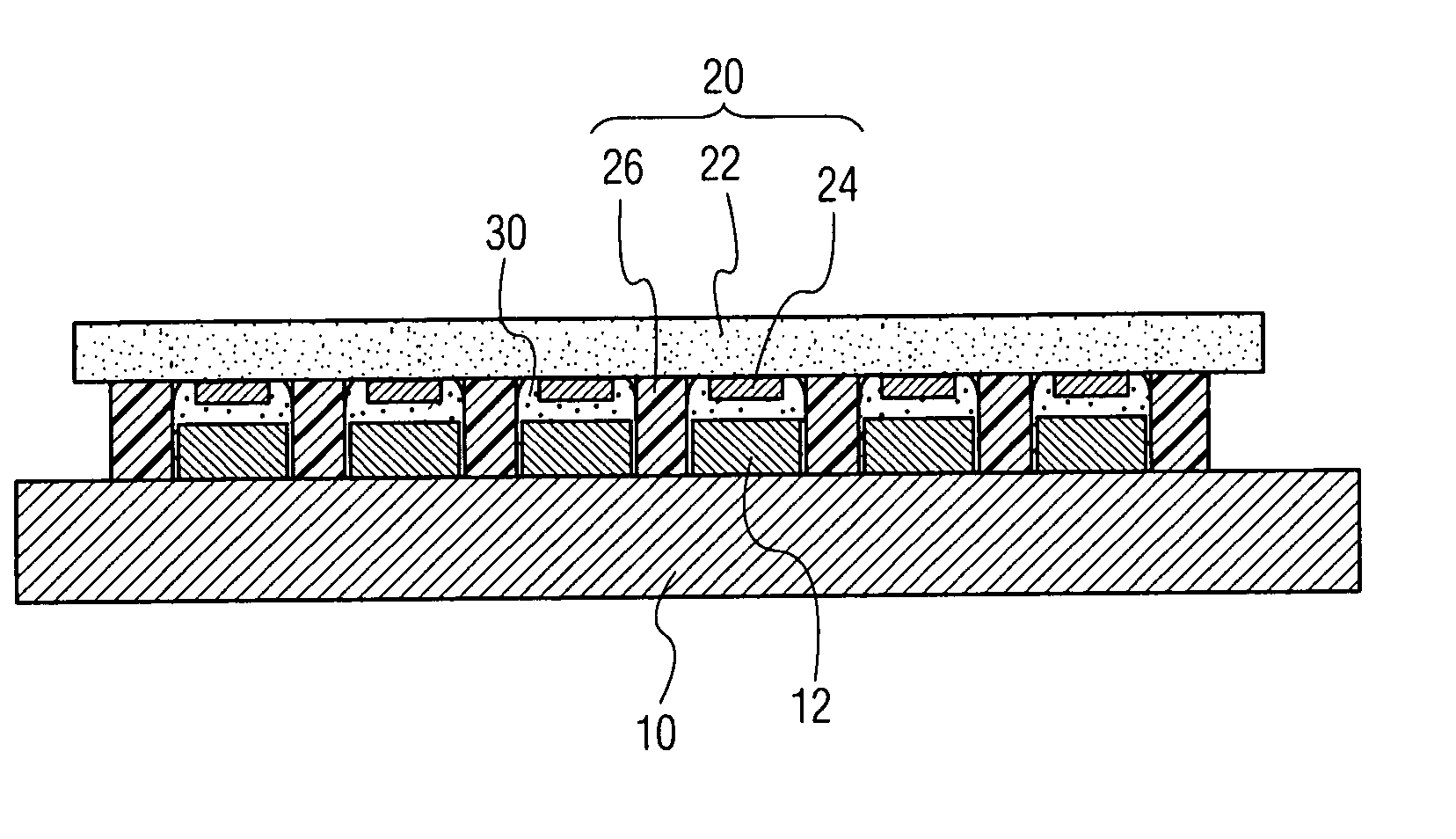
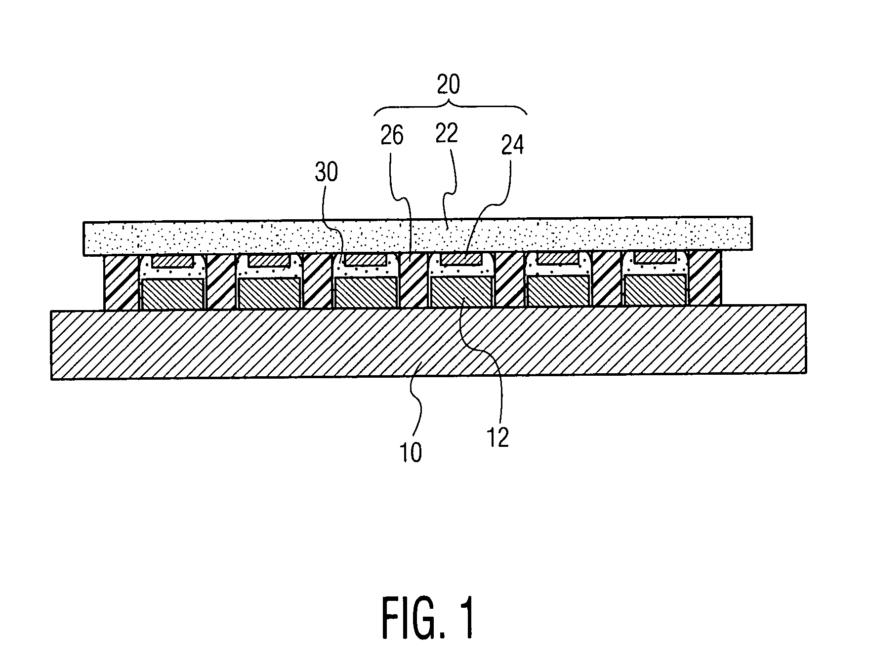
[0035]FIG. 1 is a sectional view showing an electronic circuit connecting structure in the first exemplary embodiment of the present invention. Circuit board 10 is configured in that a land (not shown) for mounting electronic parts (not shown) and conductor patterns (not shown) for connecting these parts are formed, and the first connection land 12 comprising a part of such conductor patterns is formed on surface thereof. The circuit board 10 is also preferable to be further formed with multilayer wiring, internally equipped with electronic parts or formed with passive parts and the like by a film forming method. These configurations are not subjected to any particular limitations. Electronic parts represents a general term for passive parts and semiconductor elements.

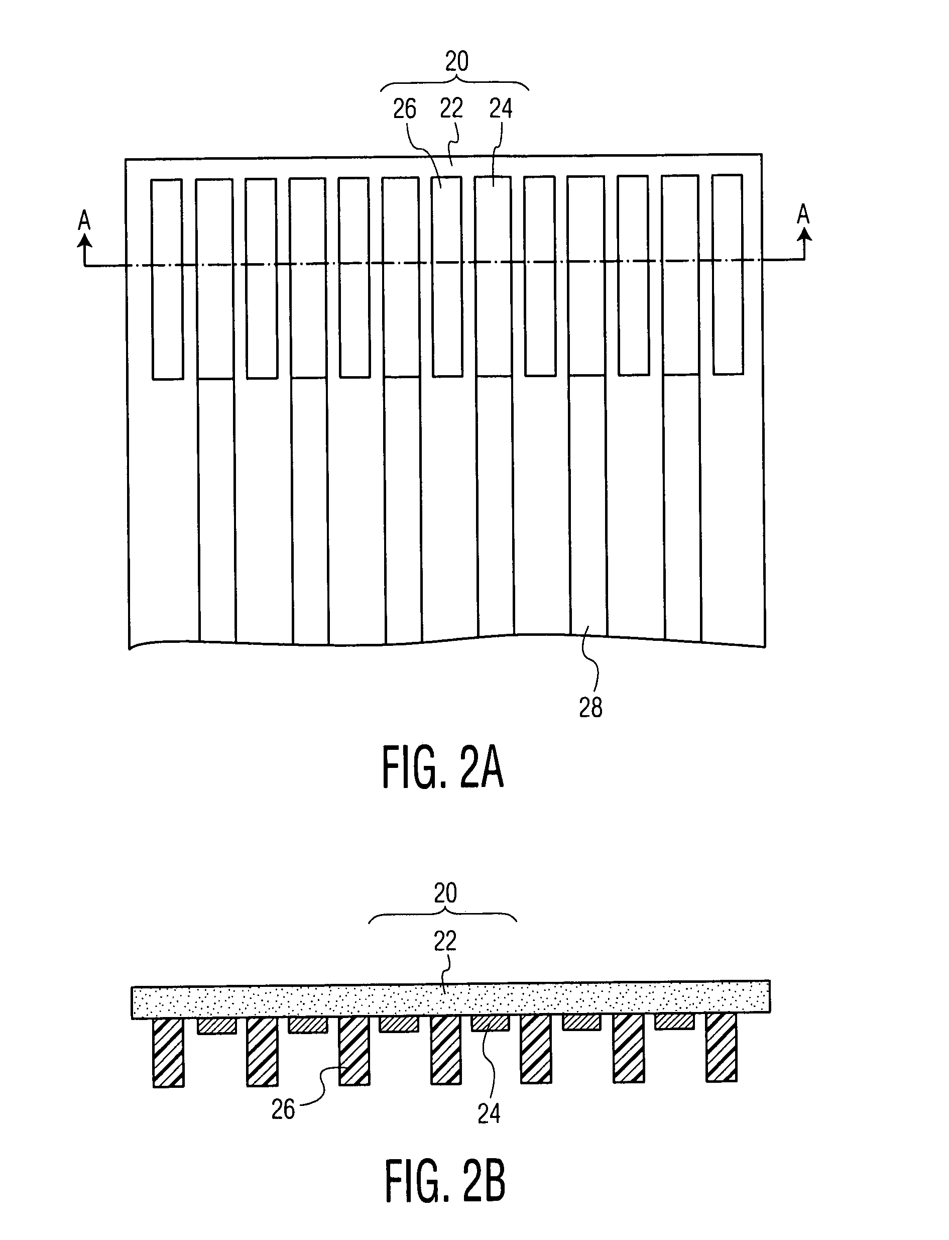
[0036]Flexible board 20 comprises substrate 22, second connection land 24 having a part of conductor patterns formed on the substrate 22, and insulating layer 26 formed so as to surround at le...

Example

Second Exemplary Embodiment

[0052]FIG. 5 is a sectional view of an electronic circuit connecting structure in the second exemplary embodiment of the present invention. In the present exemplary embodiment, the region of second connection land 150 of flexible board 200 comprises wiring conductor 130 formed corresponding to the first connection land 12 of the circuit board 10, first insulating layer 140 for covering the wiring conductor 130, region where the wiring conductor 130 is exposed via the opening formed in the first insulating layer 140, second insulating layer 160 formed so as to surround at least a part of outer periphery of the region, and second connection land 150 formed on the first insulating layer 140 and the region, which is surrounded by the second insulating layer 160.

[0053]The circuit board 10 has the first connection land 12 at least on the surface layer, the same as in the circuit board of the first exemplary embodiment. With the first connection land 12 of the ci...

Example

Third Exemplary Embodiment

[0068]An electronic circuit connecting method in the third exemplary embodiment of the present invention will be described with reference to FIG. 8A to FIG. 8G. An electronic circuit connecting structure manufactured by the electronic circuit connecting method of the present exemplary embodiment is shown in FIG. 8G, which is identical in shape with the electronic circuit connecting structure shown in FIG. 1.

[0069]Firstly, the electronic circuit connecting structure of the present exemplary embodiment will be described with reference to FIG. 8G. Circuit board 300 is formed with a land (not shown) where electronic parts (not shown) are mounted and conductor patterns (not shown) for connecting these parts, and further, the first connection land 302 having a part of such conductor patterns is formed on the surface layer thereof. The circuit board 300 is also preferable to be formed with multilayer wiring, internally equipped with electronic parts or formed with...


PUM


Abstract

A connecting structure includes a circuit board with a first connection land having a plurality of conductor patterns on the surface thereof, a second connection land disposed in a position opposite to the first connection land of the circuit board, and a flexible board including an insulating layer formed so as to surround at least a part of outer periphery of the second connection land. The first connection land and the second connection land are bonded to each other with a bonding member, and the insulating layer is thicker than the total thickness of the second connection land and the first connection land. It is possible to obtain an electronic circuit connecting structure which is free from short-circuit due to running of the bonding member such as solder even with the connecting land greatly reduced in size, and its connecting method.

Description

FIELD OF THE INVENTION[0001]The present invention relates to a connecting structure between a circuit board with electronic circuits mounted thereon and a flexible board, and its connecting method.BACKGROUND OF THE INVENTION[0002]Recently, electronic equipment has been remarkably improved in performance, reduced in thickness, weight and size. For example, in the case of a portable telephone, it is equipped with camera function and increased in size of the display screen, remaining almost unchanged in overall shape and weight as compared with a conventional type. In order to make electronic equipment higher in performance and reduced in size, it is necessary to build as many electronic circuits as possible into a limited space. For efficiently using a limited space, besides the use of only a conventional printed circuit board, the use of both flexible board and printed circuit board is increasing. In the case of using both flexible board and printed circuit board, it is necessary to ...

Claims


Application Information

Patent Timeline
IPC IPC(8): H05K1/16H05K1/14H01L21/60H05K3/32H05K3/34H05K3/36
CPCH05K3/361H05K3/363H01L24/81H01L2224/81801H05K3/321H05K3/3452H05K2201/09909H05K2201/2036H01L2924/12042H01L2924/00H05K1/14
Inventor HIGASHIDA, TAKAAKIYAMAMOTO, KENICHISUETSUGU, DAISUKENAGAOKA, MIYUKIIMANAKA, TAKASHINITTA, TOSHINARI
Owner PANASONIC CORP
Why Eureka
Try Eureka