Light emitting structure including an exposed electrode overlapping a wiring or conductive layer

a light emitting structure and exposed electrode technology, applied in the direction of electroluminescent light sources, identification means, instruments, etc., can solve the problems of low heat resistance of films with self-planarization, degradation of el elements, and inability to self-planarize, so as to improve the yield of the product, reduce the generation of trouble in the planarizing process, and facilitate the planarizing process

Inactive Publication Date: 2007-10-16
SEMICON ENERGY LAB CO LTD
View PDF40 Cites 21 Cited by
  • Summary
  • Abstract
  • Description
  • Claims
  • Application Information

AI Technical Summary

Benefits of technology

[0028]By applying the present invention, a film thickness to be deposited and an amount to be polished in a planarizing process are reduced to make the planarizing process easier. In the result, generation of trouble in the planarizing process is reduced and the yield is improved in producing. The foregoing effect that the planarizing process is made easier is effective particularly in the case of using a large-sized substrate to produce a display. Additionally, a light extraction efficiency is improved by providing a reflective film for a pixel electrode or using a film for making a surface of a second interlayer insulating film higher as a reflective film, which is provided to make planarization easier. Therefore, the present invention also has an effect that power consumption can be reduced, a sharp image can be obtained, or the like.

Problems solved by technology

However, many of films that have self-planarization such as an organic resin film have low heat resistance.
In addition, there is fear that gas is generated from the film after forming the film to cause degradation of an EL element since the film includes a volatile solvent.
However, it is often the case that many of insulating films from which no gas is generated have no self-planarization.
Therefore, a step generated due to a difference between laminated structures forming respective portions on a TFT array substrate is reflected with the result that the insulating film has an uneven surface.
In the case of forming an electrode of an EL element on the uneven insulating film, electric field becomes concentrated at an edge, which can cause acceleration of degradation of the EL element.
In addition, unevenness generated due to surface roughness generated on the insulating film cannot be completely covered with a light-emitting layer with the result that an anode and a cathode of a light-emitting element sometimes short out.

Method used


Image

  • Light emitting structure including an exposed electrode overlapping a wiring or conductive layer
  • Light emitting structure including an exposed electrode overlapping a wiring or conductive layer
  • Light emitting structure including an exposed electrode overlapping a wiring or conductive layer

Examples


embodiment mode 1

(Embodiment Mode 1)

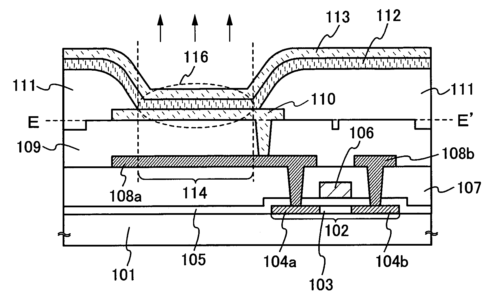
[0044]A light-emitting device according to the present invention will be described with reference to FIG. 1.

[0045]FIG. 1 is a sectional view of a light-emitting device according to the present invention. In FIG. 1, a TFT 102 for driving a light-emitting element comprising a semiconductor film that has a source (or a drain) 104a and 104b, a gate insulating film 105, and a gate electrode (a gate wiring) 106 is formed on a substrate 101. The source (or the drain) 104a of the TFT for driving the light-emitting element is connected to a wiring 108a through a contact hole provided in a first interlayer insulating film 107. The first interlayer insulating film has a surface wholly planarized.

[0046]A second insulating film 109 is formed on the first interlayer insulating film 107 and wirings 108 (108a and 108b), and the wiring 108a is connected to an electrode 110 of the light-emitting element through a contact hole provided in the second insulating film 109. While a port...

embodiment mode 2

(Embodiment Mode 2)

[0055]In the present embodiment mode, a method of manufacturing a light-emitting device that has the structure shown in FIG. 1 will be described with reference to FIGS. 4 and 5 of sectional views of a process.

[0056]The structure of a TFT for driving a light-emitting element is not particularly limited, and a known structure may be used. For example, a top-gate TFT as shown in FIG. 1 may be employed or a bottom-gate TFT may be employed. Further, a TFT that has a single-gate structure may be employed or a TFT that has a multi-gate structure may be employed. Furthermore, a TFT that has an LDD (Lightly Doped Drain) structure may be employed and a TFT that has a single-drain structure may be employed. Besides, concerning crystallinity of the semiconductor film, an amorphous semiconductor film may be employed or a crystalline semiconductor film may be employed. In this way, as long as a thin film transistor includes a semiconductor film, a gate insulating film, and a ga...

embodiments

Embodiment 1

[0071]By applying the present invention, a film thickness to be deposited and an amount to be polished can be reduced in a planarizing process to make planarization easier.

[0072]A method of manufacturing a light-emitting device, to which the present invention is applied, will be described with reference to a top view in FIG. 3 and sectional views of processes in FIGS. 6 to 11.

[0073]FIG. 3 shows a top view of a pixel portion of a light-emitting device to which the present invention is applied. In FIG. 3, a semiconductor film 401a is a semiconductor film of a thin film transistor (TFT) for driving a light-emitting element, and the semiconductor film 401a has a source (or a drain) connected to a wiring 403a through a contact hole in a region surrounded by a dotted line 406. The wiring 403a is also connected to an electrode 404 of the light-emitting element through a contact hole. In an opening of a third interlayer insulating film 405, a portion in which the wiring 403a and...


PUM


Abstract

(Object) In a light-emitting device, it is preferable that a surface of a film below a light-emitting element has flatness. Therefore, treatment such as planarization of a surface of a film is performed after forming the film. The present invention proposes a structure of a light-emitting device that can make the foregoing planarization easier.(Solving Means)The same layer as a wiring formed on a first film is used to manufacture a second film. Herewith, a portion of the first film below a light-emitting element can be prevented from being etched to form unevenness at a surface of the first film during the formation of the wiring. In addition, a surface of a third film is made higher by providing the second film to enable local planarization.

Description

TECHINICAL FIELD[0001]The present invention relates to a light-emitting device and a manufacturing method thereof, in particular, to a light-emitting device to which a structure that makes a planarization process easier is applied and a manufacturing method thereof.BACKGROUND ART[0002]Attention is paid to development of an EL display using an electroluminescence (Electro Luminescence; hereinafter, abbreviated to “EL”) element that is a light-emitting element that has characteristics such as self-light emission, wide viewing angle, high-speed response, low voltage drive, and low power consumption.[0003]An EL display is classified into a passive matrix type or an active matrix type depending on a driving method of an EL element.[0004]In an active matrix EL display, a thin film transistor (Thin Film Transistor; hereinafter, abbreviated to “TFT”) is used for driving an EL element, and generally, after forming on a substrate a driver circuit comprising a TFT, and the like, an EL element ...

Claims


Application Information

Patent Timeline
Patent Type & Authority Patents(United States)
IPC IPC(8): H01L29/04H01L31/036H01L31/0376H01L31/20G09F9/30H01L21/00H01L27/32H01L51/50H01L51/52H01L51/56H05B33/10H05B33/12H05B33/22
CPCH01L27/1248H01L51/5203H01L27/3244H01L51/56H10K59/123H10K59/12H10K59/124H10K71/00H10K2102/3026H10K59/805H10K50/805
Inventor MURAKAMI, SATOSHIMIYAGI, NORIKO
Owner SEMICON ENERGY LAB CO LTD
Why Eureka
Try Eureka