Physical realization of dynamic logic using parameterized tile partitioning

a dynamic logic and tile partitioning technology, applied in the field of semiconductor device design, can solve the problems of inability to optimize certain areas, time-consuming and error-prone design of integrated circuits using transistor synthesis methods, and inability to provide predesigned library cells, etc., and achieve the effect of reducing the number of human intervention

Inactive Publication Date: 2007-05-15
APPLE INC
View PDF4 Cites 198 Cited by
  • Summary
  • Abstract
  • Description
  • Claims
  • Application Information

AI Technical Summary

Problems solved by technology

Designing integrated circuits using transistor synthesis methods can be laborious, time-consuming, and error-prone.
This method requires extensive libraries of standard cell designs, and layout designers using a standard cell synthesis method often find that predesigned library cells are either not available or not optimal for certain areas of the design.
Accordingly, although automated standard cell synthesis methods are generally less labor-intensive than transistor synthesis methods, a substantial amount of human intervention is often required to achieve an optimized design.
Like standard cell synthesis, tile synthesis is a less laborious automatic layout method than transistor synthesis, but tile synthesis methods do not provide for design flexibility, due to limited tile design choices and fixed device sizes.
While the transistor synthesis method enables substantial design flexibility, particularly in sizing individual devices, it is labor-intensive and can result in inefficient logic partitioning and routing problems.

Method used


Image

  • Physical realization of dynamic logic using parameterized tile partitioning
  • Physical realization of dynamic logic using parameterized tile partitioning
  • Physical realization of dynamic logic using parameterized tile partitioning

Examples


Embodiment Construction

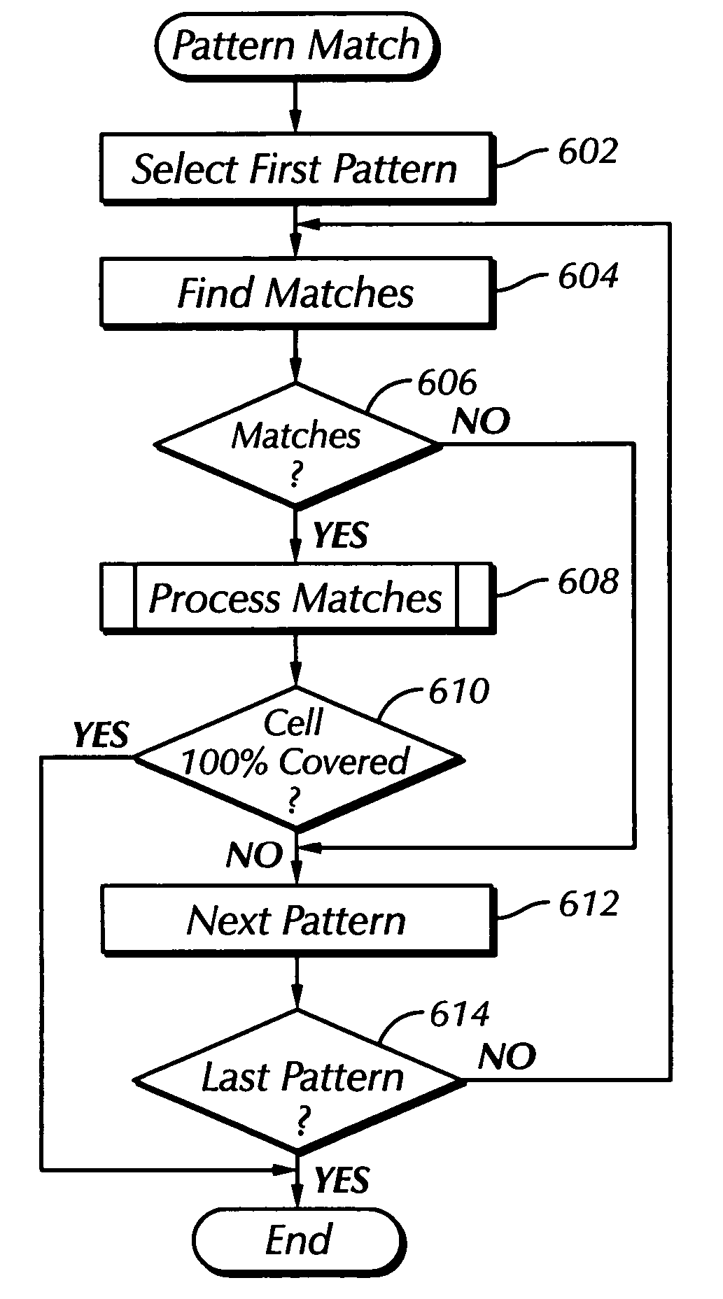
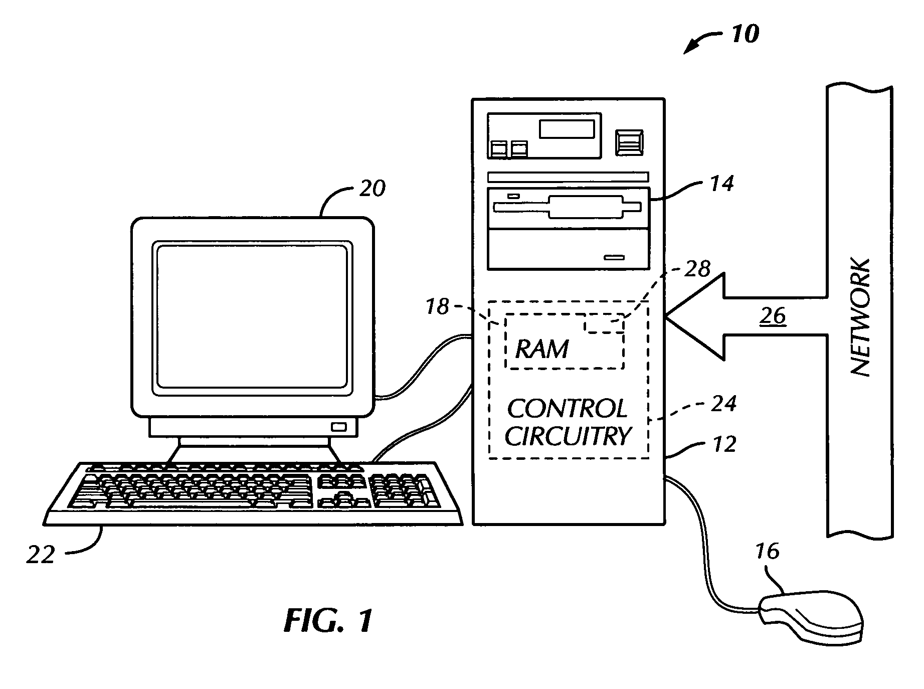
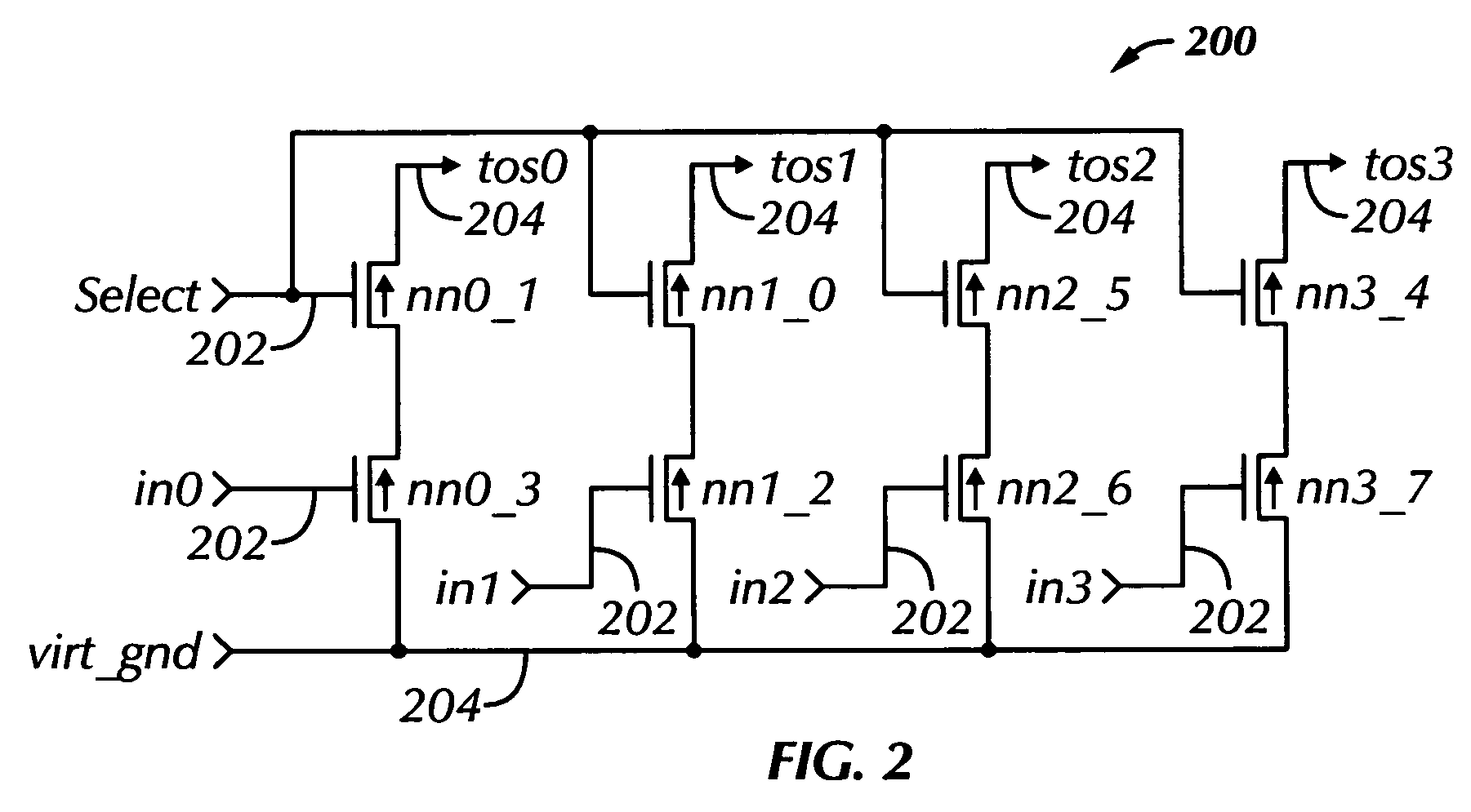
[0020]The present invention is an automatic integrated circuit layout methodology and apparatus therefore that uses a collection of parameterized tiles. This disclosure describes numerous specific details that include specific structures, circuits, and logic functions in order to provide a thorough understanding of the present invention. One skilled in the art will appreciate that one may practice the present invention without these specific details. In addition, the present invention is described herein in the context of the layout of an integrated circuit implemented in N-Nary logic. Those skilled in the art will understand that the present invention is not limited to use with N-Nary logic designs, but can be applied to any static or dynamic logic design. Notwithstanding, given that the circuit and schematic examples shown herein are circuits implemented in N-Nary logic, readers unfamiliar with N-Nary logic may find the following brief discussion of the N-Nary logic design approac...


PUM


Abstract

The matching algorithm of the layout synthesis method and apparatus disclosed locates transistor pattern matches in a design, links a parameterized tile to each identified match, and adjusts certain variable parameters of the linked parameterized tile to meet the physical design requirements of each located match. Each transistor pattern corresponds to a parameterized tile, which is an actual physical representation of the corresponding pattern and includes variable parameters, which may include transistor size. The matching algorithm locates matches in the design for an ordered list of patterns, names each located match, links the proper parameterized tile to each named match, and adjusts the tile's variable parameters as required. Transistors in the design are included in one and only one named located match.

Description

CROSS REFERENCE TO RELATED APPLICATIONS[0001]This application claims the benefits of the earlier filed U.S. Provisional Application Ser. No. 60 / 433,826, filed 16 Dec. 2002, which is incorporated by reference for all purposes into this specification.BACKGROUND OF THE INVENTION[0002]1. Field of the Invention[0003]The present invention relates to the design of semiconductor devices. More specifically, the present invention relates to the use of a transistor pattern matching algorithm to efficiently partition logic on a semiconductor device, wherein each transistor pattern corresponds to a scaleable physical realization of the transistor pattern referred to herein as a parameterized tile.[0004]2. Description of the Related Art[0005]Creating the physical representation of an integrated circuit in an automated fashion is commonly referred to as layout synthesis. The state of the art includes the following methods:[0006]Transistor Synthesis is the method of mapping each transistor in the d...

Claims


Application Information

Patent Timeline
Patent Type & Authority Patents(United States)
IPC IPC(8): G06F17/50
CPCG06F17/5068
Inventor REED, JEFFREY B.BLOMGREN, JAMES S.GLOWKA, DONALD W.OLSON, TIMOTHY A.RUDWICK, THOMAS W.
Owner APPLE INC
Why Eureka
Try Eureka