Electroluminescent device and method of manufacturing the same

a technology of electroluminescent devices and manufacturing methods, which is applied in the manufacture of electrode systems, electric discharge tubes/lamps, and discharge tubes luminescent screens, etc., can solve the problems of increasing the driving voltage of panels, deteriorating current characteristics, and affecting the operation of organic el devices

Active Publication Date: 2007-05-22
SAMSUNG DISPLAY CO LTD
View PDF9 Cites 3 Cited by
  • Summary
  • Abstract
  • Description
  • Claims
  • Application Information

AI Technical Summary

Benefits of technology

[0025]To solve the above-described problems, it is an aspect of the present invention to provide an electroluminescent (EL) device, and a method of manufacturing

Problems solved by technology

However, forming the second electrodes more thickly may deteriorate the current characteristics of an organic EL device, and may increase the driving voltage of a panel.
Further, the organic EL device may deteriorate due to electrostatic shock generated at contact portions between the second electrodes and the second elec

Method used


Image

  • Electroluminescent device and method of manufacturing the same
  • Electroluminescent device and method of manufacturing the same
  • Electroluminescent device and method of manufacturing the same

Examples


Embodiment Construction

[0049]Reference will now be made in detail to the present preferred embodiments of the present invention, examples of which are illustrated in the accompanying drawings, wherein like reference numerals refer to the like elements throughout. The embodiments are described below in order to explain the present invention by referring to the figures.

[0050]The following description of embodiments of the present invention is directed mainly to the structure of an organic EL device in which organic compounds are used as light-emitting layers. However, the present invention can be applied in the same manner to an inorganic EL device using inorganic compounds as light-emitting layers.

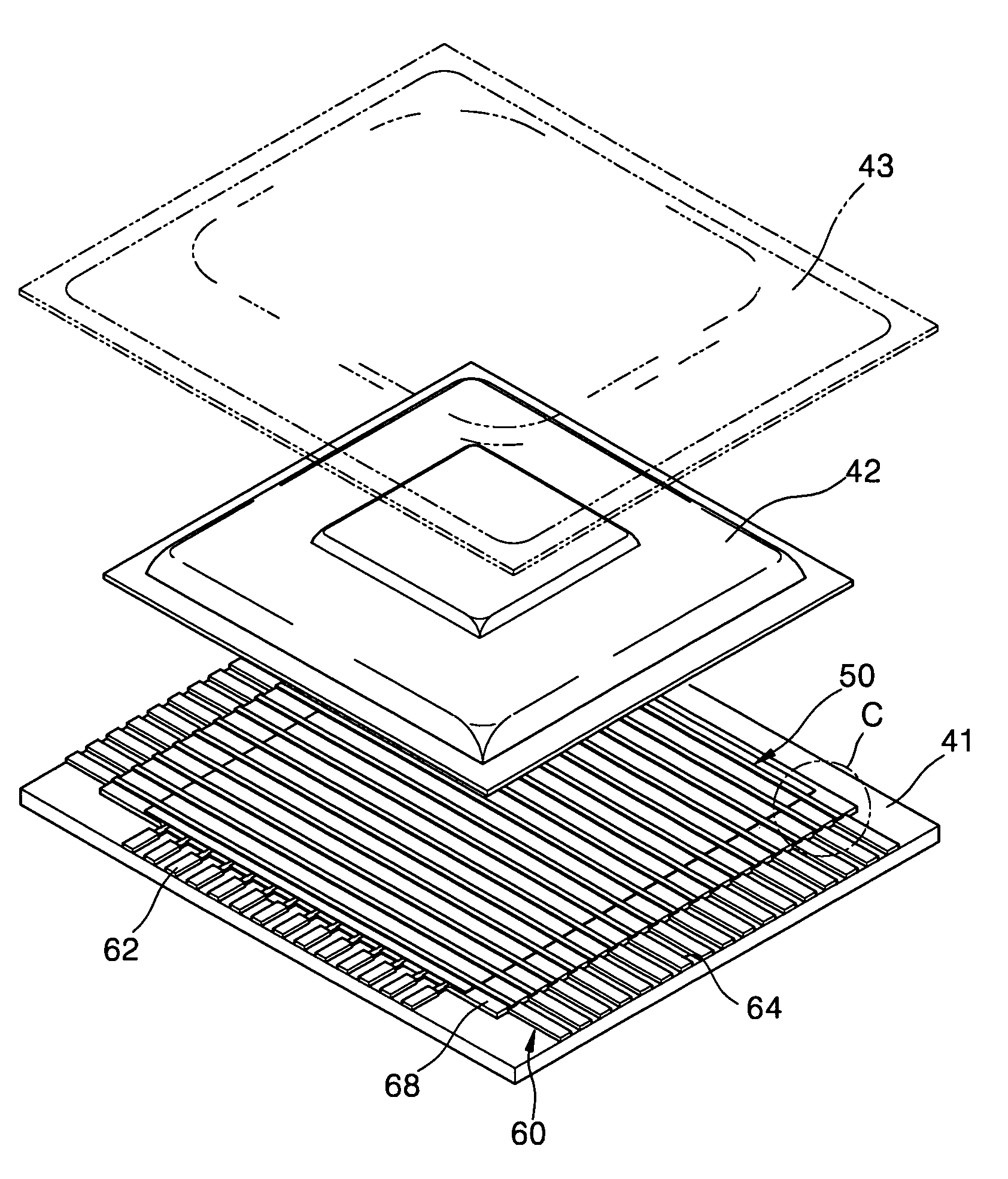
[0051]FIG. 5 is a partially exploded perspective view of an organic EL device according to an embodiment of the present invention.

[0052]Referring to FIG. 5, the organic EL device according to an embodiment of the present invention includes a transparent substrate 41, an active area 50 which is formed on the subst...


PUM


Abstract

An electroluminescent display (EL) device and a method of manufacturing the same. The EL device includes a substrate, a first electrode unit including first electrodes formed on the substrate in a predetermined pattern, and first electrode terminals connected to the respective first electrodes; a second electrode unit including second electrodes formed on the first electrodes, and second electrode terminals connected to the respective second electrodes; an emission area formed where the first electrodes intersect the second electrodes, an electroluminescent layer disposed between the first electrodes and the second electrodes in the emission area, and an outer insulating layer between the emission area and the second electrode terminals; wherein the outer insulating layer comprises an insulating material formed to contact at least an edge of the second electrode terminals facing the emission area to reduce a steepness of a step between the second electrode terminal and the substrate.

Description

CROSS-REFERENCE TO RELATED APPLICATIONS[0001]This application claims the benefit of Korean Application No. 2002-50131, filed Aug. 23, 2002, in the Korean Intellectual Property Office, the disclosure of which is incorporated herein by reference.BACKGROUND OF THE INVENTION[0002]1. Field of the Invention[0003]The present invention relates to an electroluminescent (EL) device, and, more particularly, to an improved EL device with a more secure patterning of fine electrodes, and a method of manufacturing the same.[0004]2. Description of the Related Art[0005]EL devices are self-emission type display devices, and much attention has recently been paid to the EL devices because they have advantageous features suitable for next generation devices, such as a wide viewing angle, a high contrast ratio, and a high response speed. EL devices are classified into inorganic EL devices and organic EL devices, according to the materials used for forming the light-emitting layers.[0006]In particular, st...

Claims


Application Information

Patent Timeline
IPC IPC(8): H01J17/49H01L27/32H05B33/04H05B33/26
CPCH01L27/3288H05B33/04H05B33/26H10K59/179
Inventor HEO, SE JUNKO, CHANG HEELEE, JU WON
Owner SAMSUNG DISPLAY CO LTD
Why Eureka
Try Eureka