In-situ defect monitor and control system for immersion medium in immersion lithography

a technology of defect monitor and control system, which is applied in the field of semiconductor processing, can solve the problems of limited immersion lithography, gas release by most photoresists upon exposure, and the effective wavelength of exposure radiation propagating within the immersion medium without reducing the use effect of immersion medium

Inactive Publication Date: 2007-05-29
GLOBALFOUNDRIES INC
View PDF1 Cites 44 Cited by
  • Summary
  • Abstract
  • Description
  • Claims
  • Application Information

AI Technical Summary

Benefits of technology

[0008]The following presents a simplified summary of the invention in order to provide a basic understanding of some aspects of the invention. This summary is not an extensive overview of the invention. It is intended to neither identify key or critical elements of the invention nor delineate the scope of the invention. Its purpose is merely to present some concepts of the invention in a simplified form as a prelude to the more detailed description that is presented later.

Problems solved by technology

Furthermore, utilization of an immersion medium can decrease an effective wavelength of an exposure radiation propagating within the immersion medium without changing exposure sources, lasers, lens materials, etc.
Currently, immersion lithography is limited by various characteristics of immersion mediums and the immersion lithographic process.
One significant problem encountered in immersion lithography is that most photoresists release gas upon exposure.
These bubbles can interfere with the exposure radiation resulting in scattered exposure light and potential processing defects in a substrate.

Method used


Image

  • In-situ defect monitor and control system for immersion medium in immersion lithography
  • In-situ defect monitor and control system for immersion medium in immersion lithography
  • In-situ defect monitor and control system for immersion medium in immersion lithography

Examples


Embodiment Construction

[0028]The present invention is now described with reference to the drawings. In the following description, for purposes of explanation, numerous specific details are set forth in order to provide a thorough understanding of the present invention. It may be evident, however, to one skilled in the art that one or more aspects of the present invention may be practiced with a lesser degree of these specific details. In other instances, known structures and devices may be shown in block diagram form in order to facilitate describing one or more aspects of the present invention. The following detailed description is of the best mode presently contemplated by the inventors for practicing the invention. It should be understood that the description of these aspects are merely illustrative and that they should not be taken in a limiting sense.

[0029]As used in this application, the term “component” is intended to refer to a computer-related entity, either hardware, a combination of hardware an...


PUM

PropertyMeasurementUnit
refractive indexaaaaaaaaaa
wavelengthsaaaaaaaaaa
transparentaaaaaaaaaa

Abstract

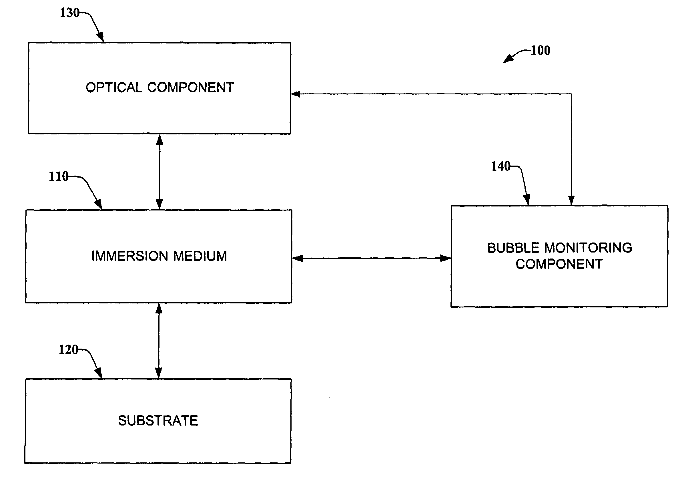
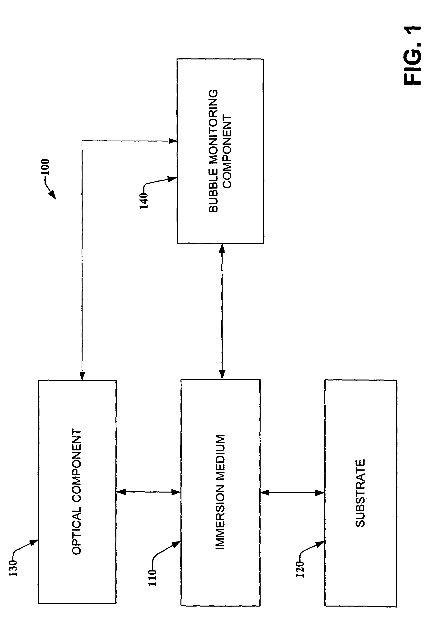
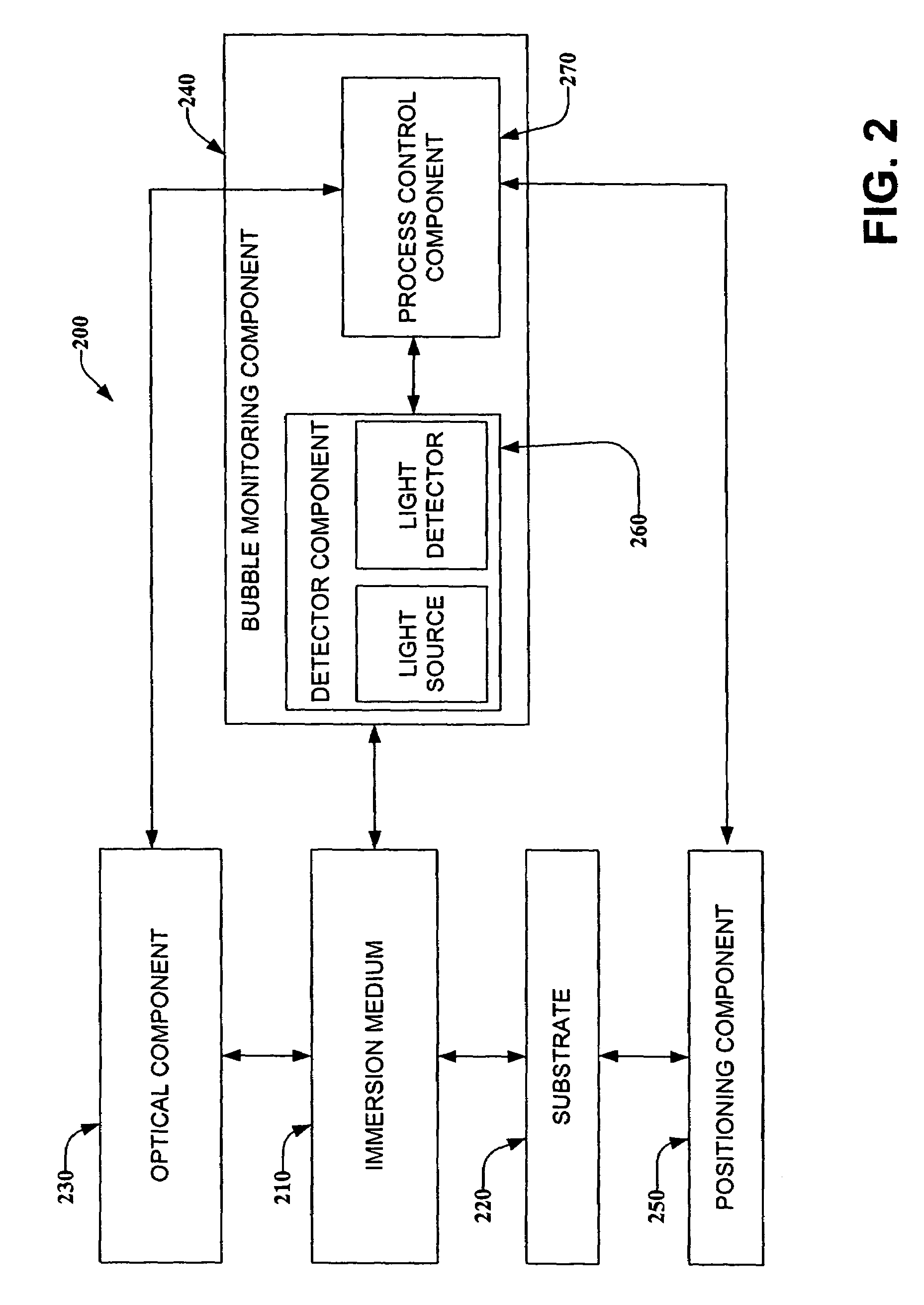
A system and method for detecting bubbles in a lithographic immersion medium and for controlling a lithographic process based at least in part on the detection of bubbles is provided. A bubble monitoring component emits an incident beam that passes through the immersion medium and is incident upon a substrate to produce a reflected and/or diffracted beam(s). The reflected and/or diffracted beam(s) is received by one or more optical detectors. The presence or absence of bubbles can be derived from information extracted by scatterometry from the reflected and/or diffracted beams. A process control component interacts with a positioning component and an optical exposure component to alter a lithographic process based at least in part on the results of the scatterometry.

Description

TECHNICAL FIELD[0001]The present invention generally relates to semiconductor processing and, more particularly, to a system and method for detecting bubbles in an immersion medium and for optimizing an immersion lithographic process based at least in part on the detection of bubbles.BACKGROUND OF THE INVENTION[0002]In the semiconductor industry, there is a continuing trend toward higher device densities. To achieve these high device densities there have been, and continue to be, efforts toward scaling down device dimensions (e.g., at sub-micron levels) on semiconductor wafers. In order to accomplish such densities, smaller feature sizes and more precise feature shapes are required. This may include width and spacing of interconnecting lines, spacing and diameter of contact holes, and surface geometry, such as corners and edges, of various features. The dimensions of and between such small features can be referred to as critical dimensions (CDs). Reducing CDs and reproducing more ac...

Claims


Application Information

Patent Timeline
Patent Type & Authority Patents(United States)
IPC IPC(8): G01N15/02
CPCG01N21/47G03F7/70341G01N2015/0011
Inventor PHAN, KHOISINGH, BHANWARRANGARAJAN, BHARATHSUBRAMANIAN, RAMKUMAR
Owner GLOBALFOUNDRIES INC
Why Eureka
Try Eureka