eFuse sense circuit

a technology of efuse and sense circuit, which is applied in the direction of static storage, digital storage, instruments, etc., can solve the problems of efuse blowing, chip manufacturing imperfectly and parts of the chip are unusable, and electronic systems often require function to be enabled, disabled or modified

Inactive Publication Date: 2007-05-29
IBM CORP
View PDF4 Cites 49 Cited by
  • Summary
  • Abstract
  • Description
  • Claims
  • Application Information

AI Technical Summary

Benefits of technology

[0014]The eFuse system reliably senses whether a particular eFuse is blown or unblown since the mirrored current is equal to the reference current (within tracking tolerances on the same chip). Theref...

Problems solved by technology

Electronic systems often require function to be enabled, disabled, or modified after semiconductor chips used in the electronic systems have been manufactured.
For a second example, sometimes chips are manufactured imperfectly and portions of the chip are unusable.
In many...

Method used


Image

  • eFuse sense circuit
  • eFuse sense circuit
  • eFuse sense circuit

Examples


Embodiment Construction

[0023]In the following detailed description of the preferred embodiments, reference is made to the accompanying drawings, which form a part hereof, and within which are shown by way of illustration specific embodiments by which the invention may be practiced. It is to be understood that other embodiments may be utilized and structural changes may be made without departing from the scope of the invention.

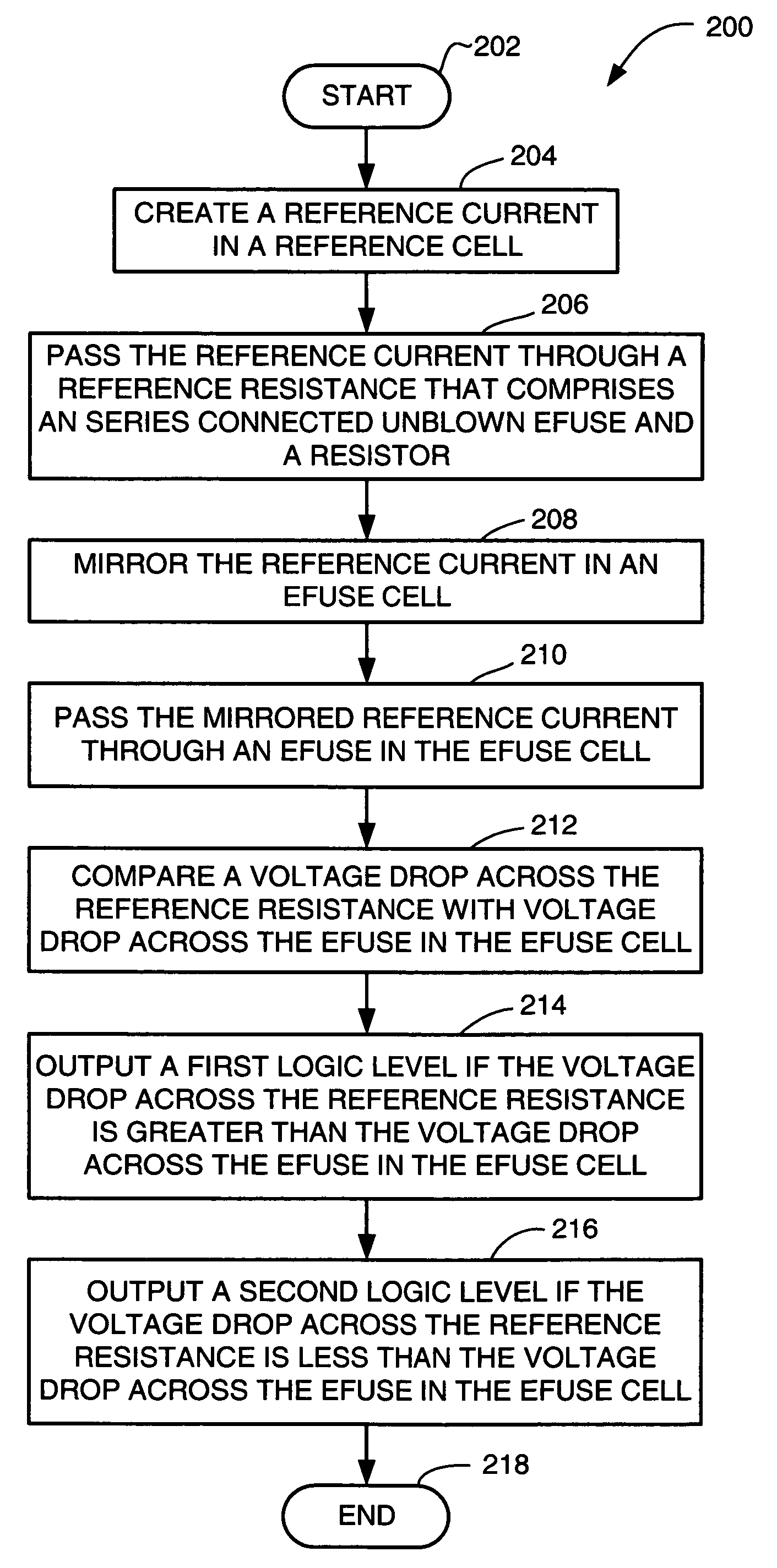
[0024]The present invention provides a method and apparatus to reliably, simply, and quickly determine if an eFuse in an eFuse system is blown or unblown.

[0025]A reference cell comprises a first circuitry configured to produce, when the first circuitry is connected to suitable voltage supplies, a reference current that passes through a reference resistance including a series connected unblown eFuse and resistor. The reference resistance is less than a resistance value of a blown eFuse on the same chip. The reference resistance is greater than a resistance of an unblown eFuse on the s...


PUM


Abstract

An eFuse reference cell on a chip provides a reference voltage that is greater than a maximum voltage produced by an eFuse cell having an unblown eFuse on the chip but less than a minimum voltage produced by an eFuse cell having a blown eFuse on the chip. A reference current flows through a resistor and an unblown eFuse in the eFuse reference cell, producing the reference voltage. The reference voltage is used to create a mirrored copy of the reference current in the eFuse cell. The mirrored copy of the reference current flows through an eFuse in the eFuse cell. A comparator receives the reference voltage and the voltage produced by the eFuse cell. The comparator produces an output logic level responsive to the voltage produced by the eFuse cell compared to the reference voltage.

Description

BACKGROUND OF THE INVENTION[0001]1. Field of the Invention[0002]This invention relates generally to eFuses (electrically programmable fuses). More specifically, this invention relates to sensing whether an eFuse is blown or not blown.[0003]2. Description of the Related Art[0004]Electronic systems often require function to be enabled, disabled, or modified after semiconductor chips used in the electronic systems have been manufactured. For example, a common chip may be designed to serve multiple applications, the chip originally having circuitry to support all of the multiple applications. After manufacture of the chip, eFuses can be blown to personalize the chip for a particular specific application. For a second example, sometimes chips are manufactured imperfectly and portions of the chip are unusable. A computer processor chip may be designed to have a 128 KB (kilobyte) cache, but testing may determine that only 64 KB of the 128 KB is functional. If the remainder of the chip is f...

Claims


Application Information

Patent Timeline
IPC IPC(8): G11C17/18
CPCG11C17/18
Inventor HOVIS, WILLIAM PAULLESLIE, ALAN JAMESPAONE, PHILSILJENBERG, DAVID W.STORINO, SALVATORE NICHOLASUHLMANN, GREGORY JOHN
Owner IBM CORP
Why Eureka
Try Eureka