Memory module, test system and method for testing one or a plurality of memory modules

a memory module and test system technology, applied in the field can solve the problems of restricting the throughput of integrated memory modules, restricting the time taken to transfer defect data, and restricting the throughput of testing integrated memory modules on a tester device, so as to achieve the effect of increasing throughput and reducing the time for testing memory modules

Inactive Publication Date: 2007-06-12
POLARIS INNOVATIONS LTD
View PDF14 Cites 155 Cited by
  • Summary
  • Abstract
  • Description
  • Claims
  • Application Information

AI Technical Summary

Benefits of technology

[0010]It is an object of the present invention to provide an integrated memory module, a test system and a method for testing memory modules by means of which the time for testing memory modules can be reduced and the throughput can thus be increased.
[0013]In this way, a memory module can be produced which makes it possible to test other memory modules, even ones of the same type. Whereas it has been customary hitherto to start the self-test operation by means of a tester device and to transfer the defect data determined to the tester device, the defect data determined are now transmitted to a further memory module which, according to the invention, is equipped with a test circuit. In this way, it is possible that memory modules can reciprocally test one another without a tester device connected thereto having to intervene in the test operation. The test circuit which has to be provided for this purpose in the integrated memory modules enables the reception of defect data from other connected memory modules and stores the defect data in the memory unit in such a way that an assignment to the respective memory modules to be tested and to the memory areas in the memory modules to be tested is possible.
[0014]It may be provided that the self-test circuit generates the addresses for storing the defect data. In this way, addresses at which the received defect data are stored can be provided in the testing memory module. In this way, it is possible, on the one hand, to avoid having to transfer, with respect to the defect data, also the addresses thereof from the tested memory modules. On the other hand, it is possible to dispense with the provision of an additional address generator circuit since the self-test circuit is already designed for the generation of address values for the self-test operation.
[0015]A data compression unit may be provided in order to compress the received defect data in a redundancy-conforming manner prior to storage in the memory element. In this way, it is possible to save memory space in the testing memory module, with the result that a larger number of memory modules connected thereto can be tested.
[0016]As an alternative, it may be provided that the test circuit is configured in such a way as to receive defect data compressed in a redundancy-conforming manner and to store them in a manner assigned to the respective addresses of the memory areas. For this purpose, an address assignment unit is preferably provided in order to generate, from the test addresses generated by the self-test circuit, memory addresses for storing the defect data compressed in a redundancy-conforming manner. The memory addresses are assigned to the memory areas in the memory modules to be tested in such a way that each of the defect data compressed in a redundancy-conforming manner can be assigned to a corresponding memory area in the memory module to be tested. In this way, it is possible to use the self-test circuit for generating the addresses to which the defect data of the tested memory modules are to be written. The address assignment unit has the function, in the case of defect data compressed in a redundancy-conforming manner, of making the addresses available in such a way that as little memory space as possible or no memory space is wasted in the memory unit.
[0025]The method according to the invention has the advantage that the self-test operation, after the start, can be carried out independently of a connected tester device since the defect data are stored in the first memory module. The first memory module thus forms that part of a tester device which receives the defect data and stores them in a defect data memory. As a result, it is possible to relieve the burden on the tester device in that defect data are transferred to the tester device only once, namely after the conclusion of the self-test operation. Since the self-test operation usually comprises a plurality of address passes in which defect data are respectively made available, the first memory module thus serves to receive the defect data, to store and to collect them in a suitable manner and to transfer them to the tester device or the defect data evaluation unit of the tester device only after the conclusion of the self-test operation. Consequently, the quantity of data to be transferred to the tester device can be considerably reduced, with the result that a larger number of memory modules can be tested simultaneously.

Problems solved by technology

This is time-consuming and considerably restricts the throughput of integrated memory modules.
Despite compression, the time taken to transfer the defect data is considerable and the throughput when testing integrated memory modules on a tester device is thus restricted.

Method used


Image

  • Memory module, test system and method for testing one or a plurality of memory modules
  • Memory module, test system and method for testing one or a plurality of memory modules

Examples


Embodiment Construction

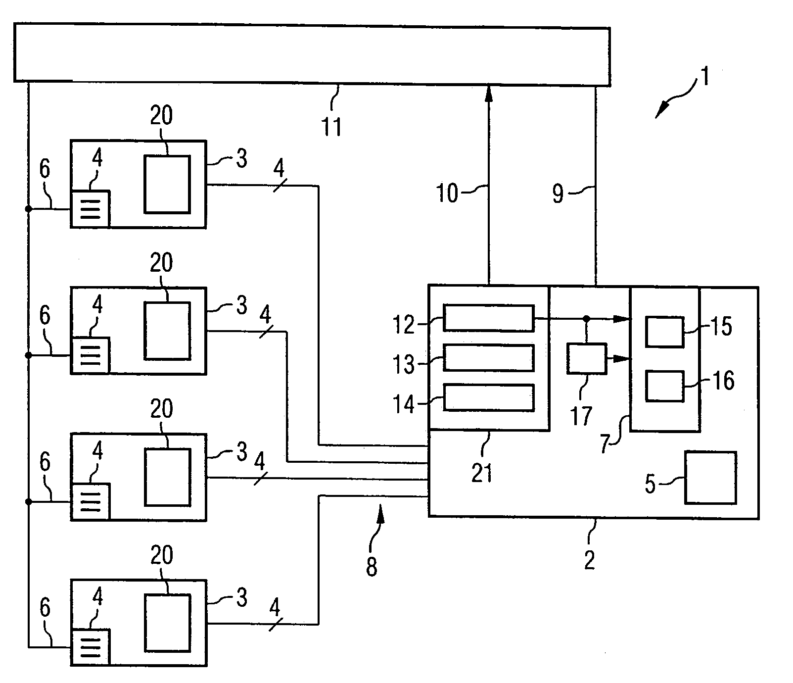
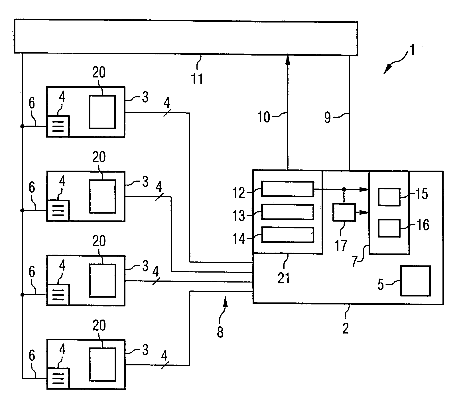
[0028]The single FIGURE shows a test system 1 according to the invention having an integrated first memory module 2 according to the invention and second memory modules 3 connected thereto. The second memory modules 3 may be both conventional memory modules to be tested and memory modules to be tested which are structurally identical to the first memory module 2. What is essential for the second memory modules 3 is that they each have a second self-test unit 4. The first memory module 2 has a first memory unit 5 and the second memory modules 3 have second memory units 20.

[0029]The self-test unit 4 serves to start a self-test in accordance with a corresponding test start command, the memory cells (not shown) of a memory unit 20 in the respective second memory module 3 in each case being tested during the self-test. Defect data which specify whether a memory cell is defective or functions without any defects are generated during the self-test.

[0030]The test start command is received b...


PUM


Abstract

The invention relates to an integrated memory module having a memory unit and a self-test circuit, the self-test circuit being embodied in such a way as to make available test data and test addresses for testing memory areas in the memory unit and to generate defect data depending on the detection of a defect, a test circuit being provided in order to receive defect data from one or a plurality of connectable memory modules to be detected, the test circuit being configured in such a way as to store the received defect data depending on addresses assigned thereto in the memory unit.

Description

CROSS-REFERENCE TO RELATED APPLICATIONS[0001]This application claims foreign priority benefits under 35 U.S.C. §119 to co-pending German patent application number 103 00 781.4, filed Jan. 11, 2003. This related patent application is herein incorporated by reference in its entirety.BACKGROUND OF THE INVENTION[0002]1. Field of the Invention[0003]The invention relates to an integrated memory module having a self-test circuit, to a test system and also to a method for testing integrated memory modules.[0004]2. Description of the Related Art[0005]In order to check integrated memory modules with regard to their functionality after the production process, they are tested. For this purpose, the integrated memory modules are connected to a tester device and a test operation is started, during which each of the memory cells of the integrated memory module is checked with regard to predetermined specifications.[0006]The memory module is tested by data being written in and subsequently read out...

Claims


Application Information

Patent Timeline
Patent Type & Authority Patents(United States)
IPC IPC(8): G01R31/28G11C29/40
CPCG11C29/40G11C2029/0405G11C2029/1208G11C2029/2602
Inventor OHLHOFF, CARSTENBEER, PETER
Owner POLARIS INNOVATIONS LTD
Why Eureka
Try Eureka