Cooler for cooling both sides of semiconductor device

a cooling device and semiconductor technology, applied in semiconductor/solid-state device details, lighting and heating apparatus, laminated elements, etc., can solve the problem of large temperature variation of semiconductors, achieve uniform heat dissipation, reduce heat dissipation capability variation, and uniform heat dissipation

Active Publication Date: 2007-06-19
DENSO CORP
View PDF11 Cites 19 Cited by
  • Summary
  • Abstract
  • Description
  • Claims
  • Application Information

AI Technical Summary

Benefits of technology

[0009]An object of the present invention is to provide a cooler using a coolant for cooling both sides (top and bottom surfaces) of a semiconductor device, wherein the variation of pressing force on flat cooling tubes holding a semiconductor device is reduced, thereby uniformly dissipating the heat generated by the semiconductor device (i.e. semiconductor chip or module) and moreover reducing the variation of heat dissipation capability depending upon the position of semiconductor device. The above-mentioned uniform heat dissipation capability is achieved by a simple structure.

Problems solved by technology

However, the cooler as disclosed in JP2001-320005A has a disadvantage that the temperature of the semiconductor may vary widely, even when the heat generated by the semiconductor devices is even.

Method used


Image

  • Cooler for cooling both sides of semiconductor device
  • Cooler for cooling both sides of semiconductor device
  • Cooler for cooling both sides of semiconductor device

Examples


embodiment 1

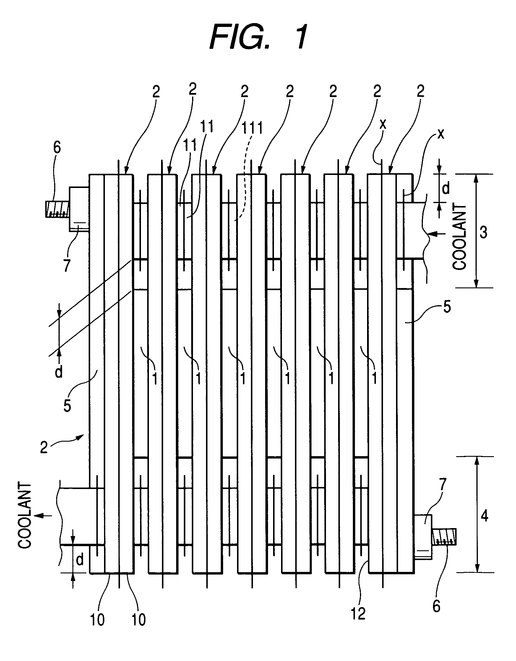
[0039]FIG. 1 is an elevational view of a cooler for cooling a plurality of semiconductor devices of the present invention which comprises: six semiconductor modules 1; seven flat cooling tubes 2; an inlet header 3; an outlet header 4; two holding plates 5; two through bolts 6; and two nuts 7. Here, holding plates 5, bolts 6 and nuts 7 construct a pressing mechanism.

[0040]The six semiconductor modules 1 constitute arms of a three-phase inverter. The semiconductor module 1 comprises: a semiconductor chip, i.e. a transistor in this embodiment; and a pair of main electrode plates attached to each surface of the semiconductor chip. The semiconductor chip and the main electrode plates are molded in resin in a flat shape, with signal terminals and control electrode terminals extending therefrom. Concretely, a part of the main electrode plate on the top surface of the semiconductor chip is recessed in order to expose conductive pads for a control electrode as well as communication electrode...

embodiment 2

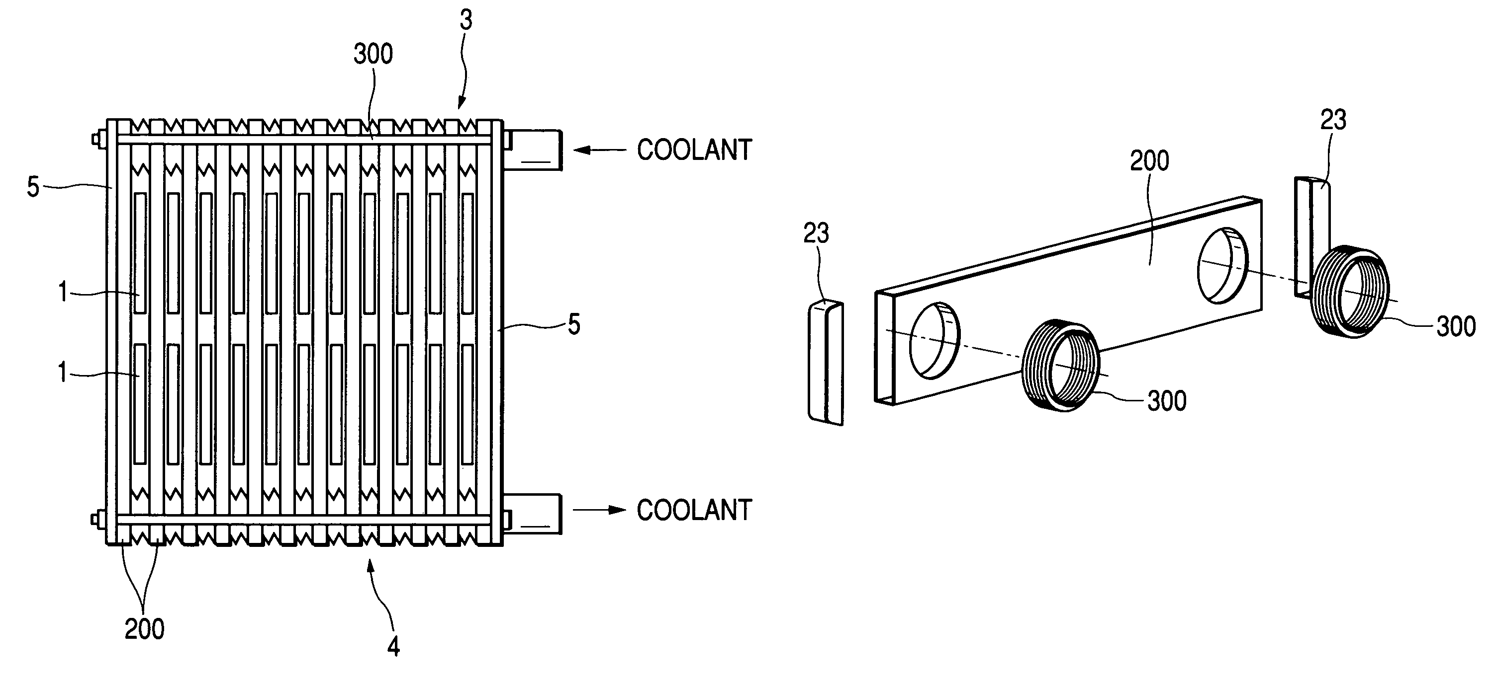
[0054]FIG. 10 is an elevational view of the cooler of Embodiment 2, while FIG. 11 is an exploded perspective view of the flat cooling tube 200 and a part of the inlet and outlet headers 3 and 4 of FIG. 10. The flat cooling tube 200 is an extruded metal plate, and caps 23 are brazed at both ends. Further, bellows 300 are brazed to holes bored at right and left hand ends of the flat cooling tube 200, thereby constructing the inlet and outlet headers 3 and 4. The bellows 300 is preferable because it is more flexible along the stacking direction than the diaphragm of Embodiment 1. Accordingly, the dimensional tolerances of the components are absorbed more easily than Embodiment 1, thereby enabling closer contact of the flat cooling tube 200 to the semiconductor module 1 and therefore, thereby transferring heat better from the semiconductor module 1 to the flat cooling tube 200, without applying excessively strong force on the semiconductor module.

[0055]FIG. 12 is an enlarged view of the...

embodiment 3

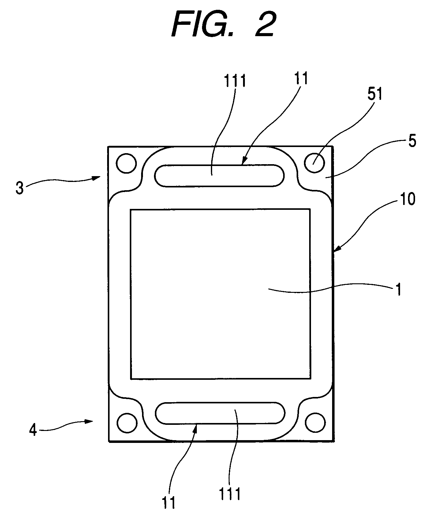
[0057]Another embodiment of this invention is explained below in reference to FIG. 14. FIG. 14 shows a variant of the embodiment previously shown in FIG. 1, enlarging a part proximate to the header 3 only. Here metal plates 10 in FIG. 1 of the embodiment 1 are, here in FIG. 14, shown as press-formed metal plates 10a and 10b, expressed simply as lines omitting their thicknesses.

[0058]The feature of this embodiment resides in that the metal plates 10a and 10b are formed in different shapes from each other. The metal plates 10a and 10b are joined, for example, by brazing similarly to the embodiment 1.

[0059]The metal plates 10a and 10b have holes 111 similarly to the metal plates 10 of the embodiment 1. The metal plate 10a has a diaphragm disk 12a around the connecting pipe portion 11, while the metal plate 10b has a diaphragm disk 12b correspondingly.

[0060]In this embodiment, each of the diaphragm disks 12a and 12b consists of four rings formed coaxially. The rings of the two diaphragm...


PUM


Abstract

An object of the present invention is to provide a cooler for cooling both sides (top and bottom surfaces) of a semiconductor device, wherein the variation of pressing force on flat cooling tubes holding a semiconductor device is reduced, thereby uniformly dissipating the heat generated by the semiconductor device. When the holding plates press the flat cooling tubes and semiconductor modules by tightening the nut, the dimensional tolerances in the stacking direction are absorbed by the deformable portions in the inlet and outlet headers. A spacer may be employed inside the flat cooling tubes in order to suppress the deformation of the flat cooling tubes along the stacking direction.

Description

BACKGROUND OF THE INVENTION[0001]1. Field of the Invention[0002]The present invention relates to a cooler for cooling both sides (top and bottom surfaces) of a semiconductor device.[0003]2. Description of the Related Art[0004]There is disclosed in JP2001-320005A one of the conventional coolers for cooling both sides of a semiconductor device, which comprises: a plurality of flat cooling tubes each of which has heat-absorbing surfaces for contacting the surfaces of semiconductor modules and one or more channels for passing a coolant and is disposed alternately with the semiconductor module; an inlet header which is connected with one ends of the flat cooling tubes and supplies the flat cooling tube with the coolant; an outlet header which is connected with the other ends of the flat cooling tubes and collects the coolant from the flat cooling tubes; and a pressing mechanism (e.g., bolt and nut) for pressing the flat cooling tubes which hold the semiconductor devices from both sides o...

Claims


Application Information

Patent Timeline
Patent Type & Authority Patents(United States)
IPC IPC(8): F28F9/013H01L23/40F28F3/12H01L23/473
CPCF28F3/12H01L23/473H01L2924/0002H01L2924/00
Inventor SAKAI, YASUYUKI
Owner DENSO CORP
Why Eureka
Try Eureka