Spin transfer magnetic elements with spin depolarization layers

Inactive Publication Date: 2007-06-19
SAMSUNG SEMICON
View PDF5 Cites 172 Cited by
  • Summary
  • Abstract
  • Description
  • Claims
  • Application Information

AI Technical Summary

Problems solved by technology

Although the spin transfer effect functions as a switching mechanism for the conventional magnetic elements 10 and 10′, complications arise when synthetic antiferromagnetic structures, such as Co / Ru / Co, are used as pinned layers or free layers.

Method used


Image

  • Spin transfer magnetic elements with spin depolarization layers
  • Spin transfer magnetic elements with spin depolarization layers
  • Spin transfer magnetic elements with spin depolarization layers

Examples


first embodiment

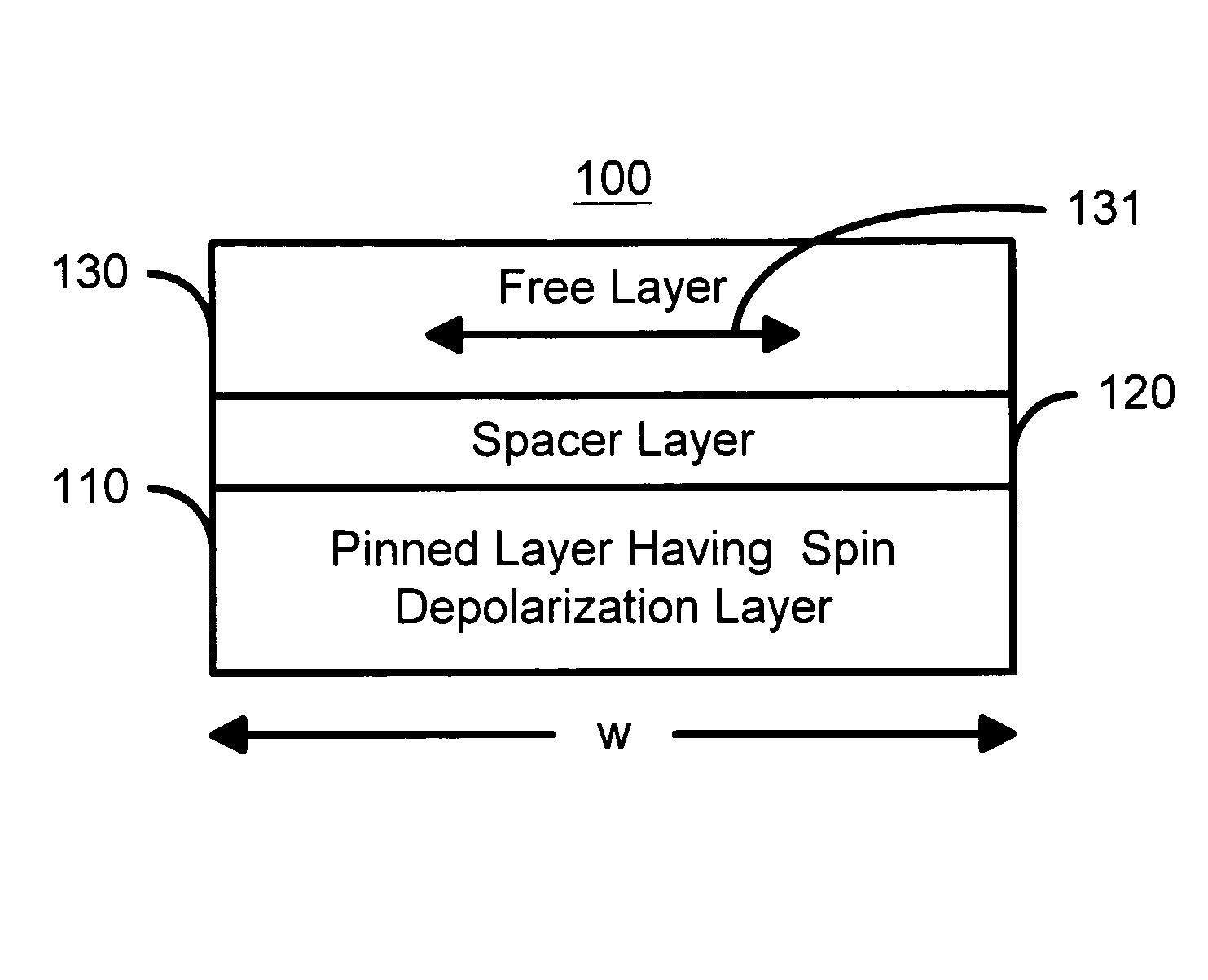
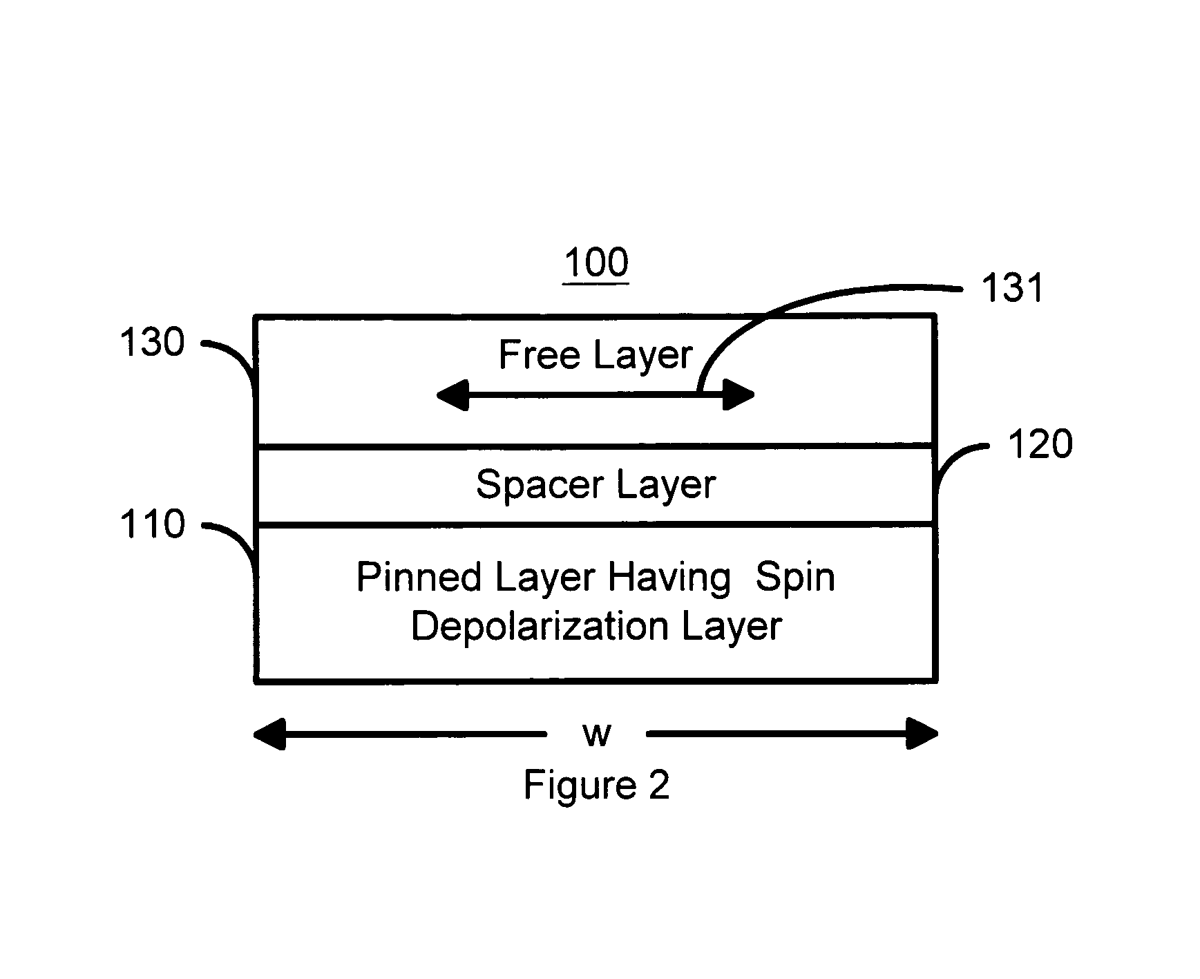
[0023]To more particularly illustrate the method and system in accordance with the present invention, refer now to FIG. 2, depicting a magnetic element 100 in accordance with the present invention having a synthetic antiferromagnetic pinned layer with at least one spin depolarization sublayer. The magnetic element 100 includes a free layer 130, a spacer layer 120, and a pinned layer 110 including at least one spin depolarization layer (SPDL). The magnetic element 100 generally also includes an AFM layer (not shown) used to pin the magnetization of the pinned layer 110, as well as seed layers (not shown) and capping layers (not shown). Furthermore, the magnetic element 100 is configured such that the free layer 130 can be written using spin transfer. Thus, the direction of the magnetization 131 of the free layer 130 can be switched using spin transfer. Consequently, in a preferred embodiment, the lateral dimensions, such as the width w, of the free layer 130 are thus small, in the ra...

second embodiment

[0029]FIG. 3B depicts a magnetic element in accordance with the present invention having a synthetic antiferromagnetic pinned layer with at least one spin depolarization sublayer. The magnetic element 100″ includes a pinned layer 110″, a spacer layer 120″ and a free layer 130″. The spacer layer 120″ and the free layer 130″ correspond to the spacer layer 120 and the free layer 130 depicted in FIG. 2. Referring back to FIG. 3B, the magnetic element 100″ is configured such that the free layer 130″ can be written using spin transfer. Thus, the direction of the magnetization 131″ of the free layer 130″ can be switched using spin transfer. Consequently, in a preferred embodiment, the lateral dimensions, such as the width w, of the free layer 130″ are thus small, in the range of a few hundred nanometers and preferably less than two hundred nanometers. In addition, some difference is preferably provided between the lateral dimensions to ensure that the free layer 130″ has a particular easy ...

third embodiment

[0032]FIG. 3C depicts a magnetic element in accordance with the present invention having reduced reflected electrons having opposing torques due to reflection at different interfaces. The magnetic element 100′″ includes a pinned layer 110′″, a spacer layer 120′″ and a free layer 130′″. The spacer layer 120′″ and the free layer 130′″ correspond to the spacer layer 120 and the free layer 130 depicted in FIG. 2. Referring back to FIG. 3C, the magnetic element 100′″ is configured such that the free layer 130′″ can be written using spin transfer. Thus, the direction of the magnetization 131′″ of the free layer 130′″ can be switched using spin transfer. Consequently, in a preferred embodiment, the lateral dimensions, such as the width w, of the free layer 130′″ are thus small, in the range of a few hundred nanometers and preferably less than two hundred nanometers. In addition, some difference is preferably provided between the lateral dimensions to ensure that the free layer 130′″ has a ...


PUM


Abstract

A method and system for providing a magnetic element is disclosed. The method and system include providing a free layer, a spacer layer, and a pinned layer. The free layer is ferromagnetic and has a free layer magnetization. The spacer layer is nonmagnetic and resides between the pinned and free layers. The pinned layer includes first and second ferromagnetic layers having first and second magnetizations, a nonmagnetic spacer layer, and a spin depolarization layer. Residing between the first and second ferromagnetic layers, the nonmagnetic spacer layer is conductive and promotes antiparallel orientations between the first and second magnetizations. The spin depolarization layer is configured to depolarize at least a portion of a plurality of electrons passing through it. The magnetic element is also configured to allow the free layer magnetization to change direction due to spin transfer when a write current is passed through the magnetic element.

Description

FIELD OF THE INVENTION[0001]The present invention relates to magnetic memory systems, and more particularly to a method and system for providing an improved magnetic element that employs a spin transfer effect in switching.BACKGROUND OF THE INVENTION[0002]FIGS. 1A and 1B depict conventional magnetic elements 10 and 10′. The conventional magnetic element 10 is a spin valve and includes a conventional antiferromagnetic (AFM) layer 12, a conventional pinned layer 14, a conventional conductive spacer layer 16 and a conventional free layer 18. Other layers (not shown), such as seed or capping layer may also be used. The conventional pinned layer 14 and the conventional free layer 18 are ferromagnetic. Thus, the conventional free layer 18 is depicted as having a changeable magnetization 19. The conventional conductive spacer layer 16 is nonmagnetic. The AFM layer 12 is used to fix, or pin, the magnetization of the pinned layer 14 in a particular direction. The magnetization of the free la...

Claims


Application Information

Patent Timeline
Patent Type & Authority Patents(United States)
IPC IPC(8): H01L29/76G11C11/00G11C11/16
CPCG11C11/16
Inventor HUAI, YIMINGNGUYEN, PAUL P.
Owner SAMSUNG SEMICON
Why Eureka
Try Eureka