Integrated circuit package with optimized mold shape

a technology of integrated circuits and molds, applied in the direction of semiconductor devices, semiconductor/solid-state device details, electrical devices, etc., to achieve the effect of increasing flexibility and reducing stiffness of said packages

Inactive Publication Date: 2007-06-19
NOKIA CORP
View PDF9 Cites 119 Cited by
  • Summary
  • Abstract
  • Description
  • Claims
  • Application Information

AI Technical Summary

Benefits of technology

[0009]The invention overcomes these problems by providing an integrated circuit package wherein said mold is provided with reduced stiffness at areas located substantially at one of said interconnection elements providing increased flexibility of said package at said areas compared to other areas of said package.
[0010]In case a consumer electronic device, or a mobile communication equipment is dropped, or subject to any other shock, the printed wiring board (PWB) bends. The integrated circuit component (IC) tries to follow the deformation of the PWB. Typically, the package of the IC is much stiffer than the PWB. This causes high stress to the connection and interconnection elements, especially in the corner and edge areas of a package, which causes them to fail first. By providing areas within said mold with reduced stiffness, the stress on the connection and interconnection elements may be reduced, and the component reliability may be improved. This is also the case in other conditions, such as bending and thermal cycling.

Problems solved by technology

This causes high stress to the connection and interconnection elements, especially in the corner and edge areas of a package, which causes them to fail first.

Method used


Image

  • Integrated circuit package with optimized mold shape
  • Integrated circuit package with optimized mold shape
  • Integrated circuit package with optimized mold shape

Examples


Embodiment Construction

Reference Numbers

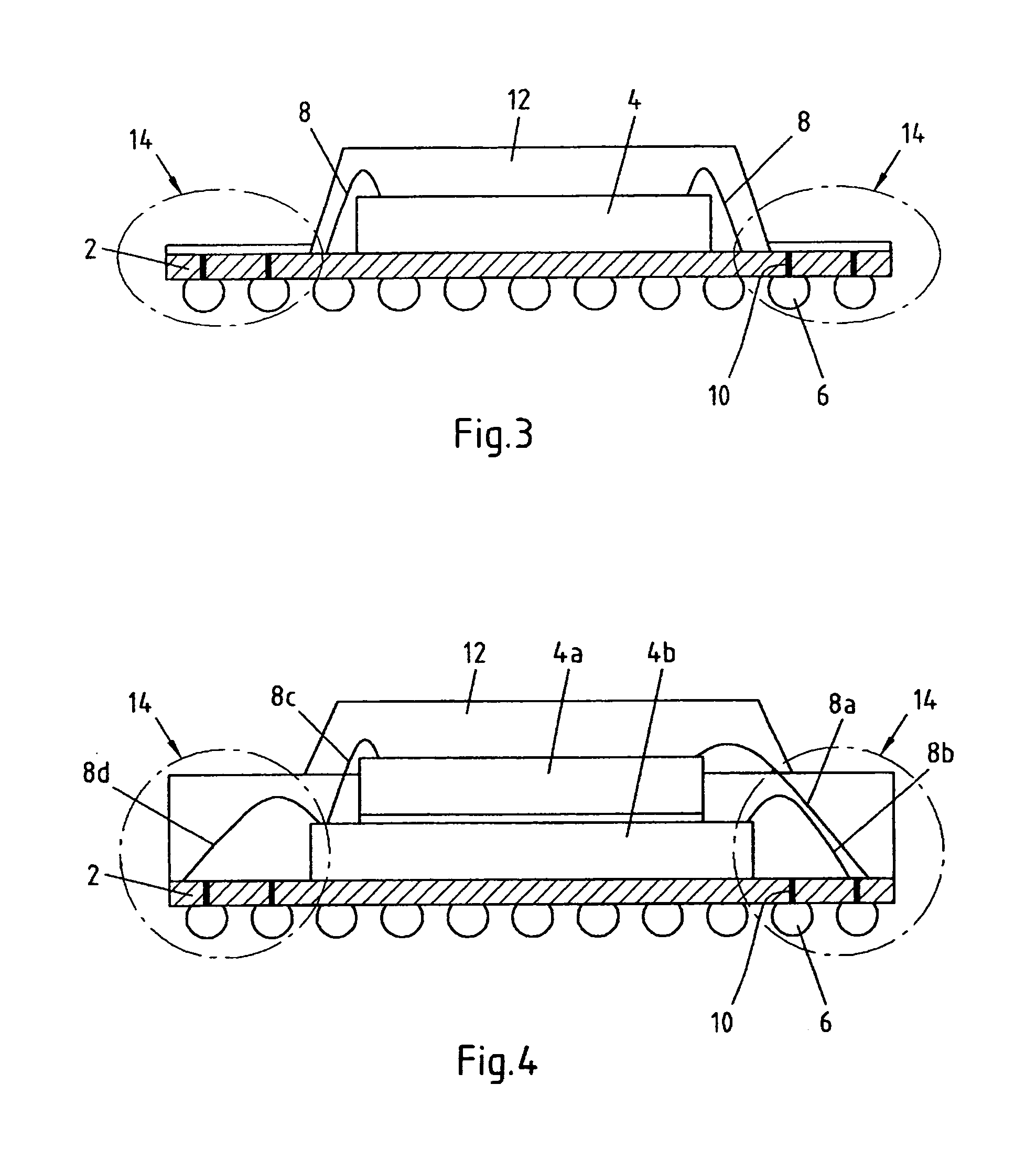
[0040]2 substrate[0041]4 die[0042]6 solder balls[0043]8 bonding wire[0044]10 vias[0045]12 mold[0046]14 area of reduce stiffness[0047]16 printing wiring board[0048]20 provide substrate[0049]22 provide die[0050]24 provide ball grid array and flexible bond ribbons and interconnect die with ball grid array[0051]26 encapsulate package by molding[0052]28 form encapsulation

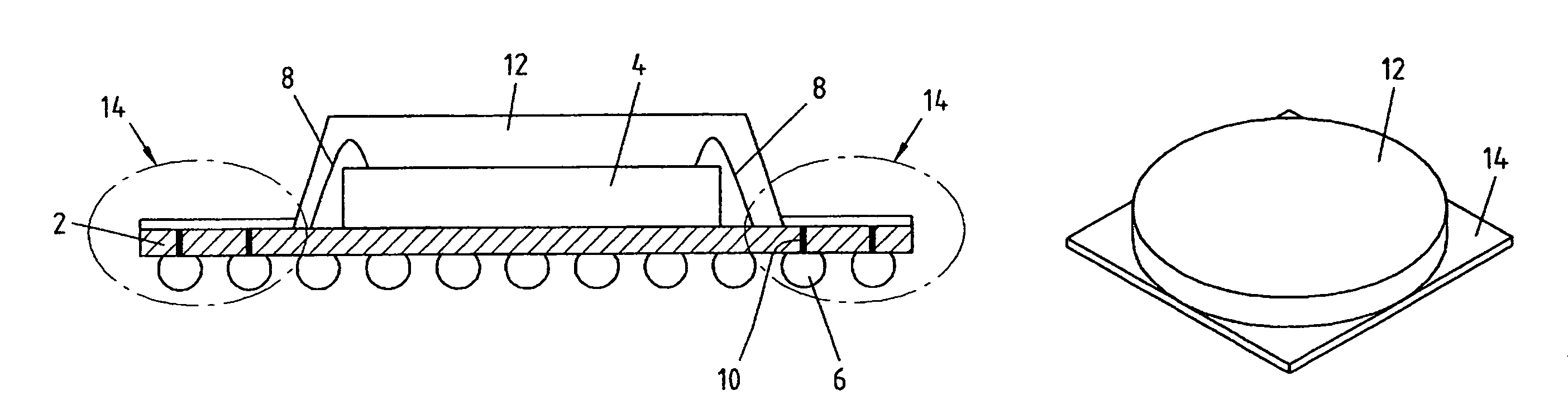
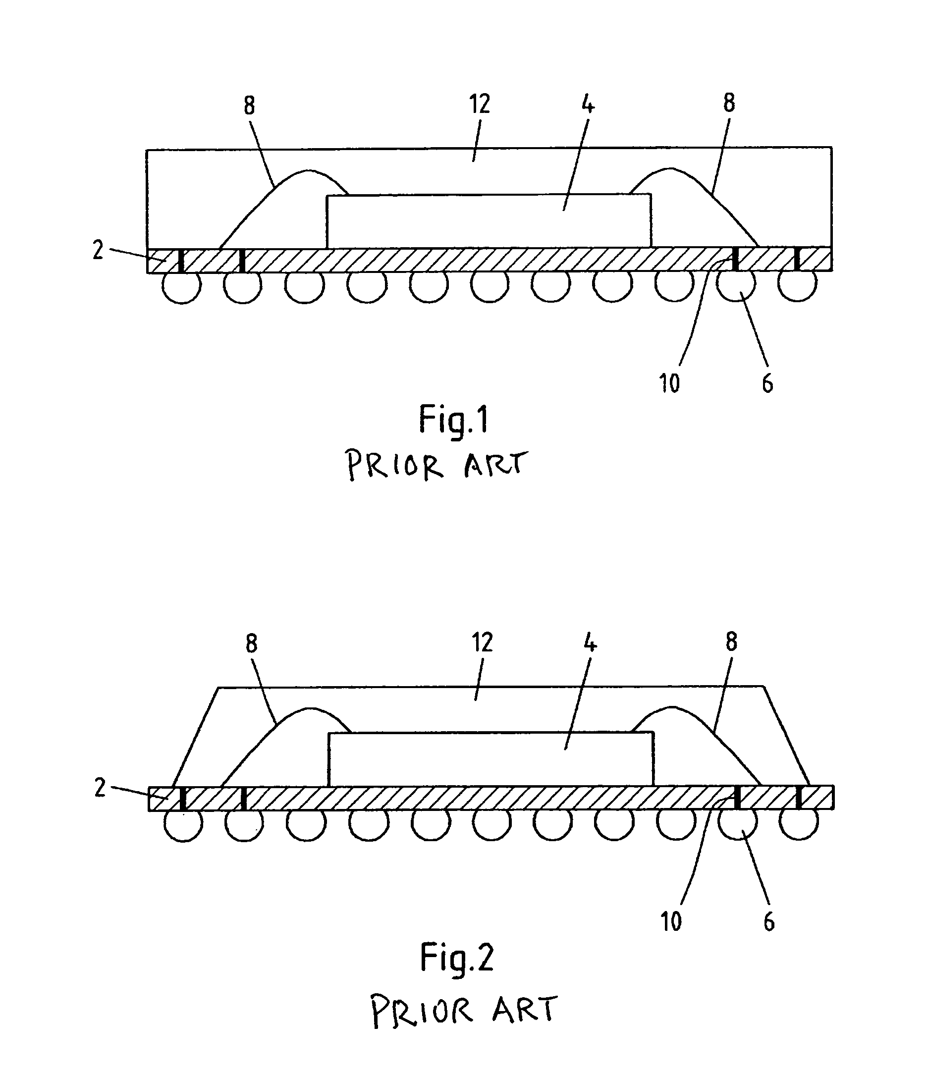
[0053]FIG. 1 depicts an integrated circuit package comprised of a substrate 2, a die 4, solder balls 6, bonding wires 8, via connections 10, and a mold 12.

[0054]The die 4 comprises the integrated circuit. The die is encapsulated onto said substrate 2 by said mold 12. Connection pins of said die 4 are connected to via connections 10 by bonding wires 8. The via connections 10 connect the bonding wires 8 with the solder balls 6. The depicted integrated circuit package is unnecessarily rigid in terms of stiffness, which will increase mechanical stress on the interconnections when mechanical stress is applied...


PUM


Abstract

The invention relates to an integrated circuit package, in particular an integrated chip size package or an integrated chip scale package, comprising a substrate carrying a die, and connection elements, interconnection elements, connecting pins of said die with said connection elements, and a mold encapsulating said die on said substrate. To increase reliability and to reduce failure due to deformation stress, the invention provides said mold with reduced stiffness at areas located substantially at one of said interconnection elements providing increased flexibility of said package at said areas compared to other areas of said package.

Description

FIELD OF THE INVENTION[0001]The invention relates to an integrated circuit package, in particular ball grid array package or a land grid array package, comprising a substrate carrying a die and connection elements, interconnection elements connecting pins of said die with said connection elements, and a mold encapsulating said die in said substrate.[0002]The invention also relates to a method for manufacturing such an integrated circuit package, wherein a substrate is provided, a die is placed on said substrate, connection elements are placed on said substrate, interconnection elements connecting pins of said die with said connection elements are provided, and a mold encapsulating said die on said substrate is provided.[0003]Eventually, the invention relates to the use of such an integrated circuit package.BACKGROUND[0004]Electronic components are subject to miniaturizing. Therefore, electronic components of these products need to be ever smaller and lighter. As a result, more and m...

Claims


Application Information

Patent Timeline
Patent Type & Authority Patents(United States)
IPC IPC(8): H01L23/04H01L23/28H01L23/31H01L25/10
CPCH01L23/3107H01L23/3128H01L25/105H01L2224/32145H01L2224/48091H01L2224/48145H01L2224/73265H01L2924/15311H01L2924/1815H01L2924/00014H01L2224/32225H01L2224/48227H01L2924/00012H01L24/48H01L2225/1023H01L2225/1058H01L2924/00H01L24/73H01L2224/45014H01L2924/14H01L2924/181H01L2224/45015H01L2924/207
Inventor HUSSA, ESA
Owner NOKIA CORP
Why Eureka
Try Eureka