
Method and apparatus for selective scan chain diagnostics

a scan chain and diagnostic method technology, applied in the direction of instruments, measurement devices, computing, etc., can solve the problem that human error is often part of misdiagnosis of parts, and achieve the effect of significantly reducing the time required to diagnose parts

Inactive Publication Date: 2007-06-19
GOOGLE LLC
View PDF14 Cites 25 Cited by
  • Summary
  • Abstract
  • Description
  • Claims
  • Application Information

AI Technical Summary

Benefits of technology

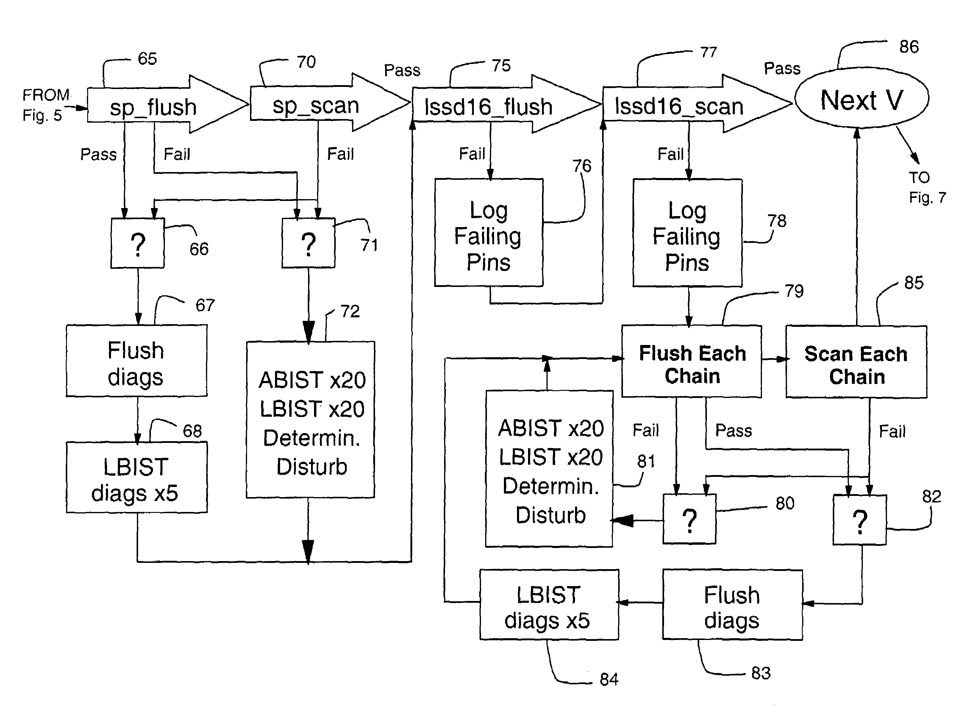
The present invention is a system and method for automatically diagnosing large amounts of electronic chips using existing scan chain diagnostic methods. The system uses an algorithm to determine the test application protocol and order of execution, and the appropriate scan diagnostic techniques to perform based on prior and combined test results. The system collects the results of the scan diagnostics and analysis of the data to determine which devices, to send to PFA. The method includes a flush test executed for the scan chain under test and wherein the flush test diagnostics for the flush test are recorded. The method also includes a scan test executed for the scan chain under test and wherein further test diagnostics are recorded in the event either or both the flush test or the scan test fails. The recorded flush test diagnostics and further test diagnostics are then analyzed to identify a call to one or more probable failed or failing shift register latches in the tested scan chain. The method may also include different voltage levels to determine the sensitivity of the scan chain being tested to varying voltage levels. The technical effects of this invention include reducing human error, reducing the time required to diagnose parts, and increasing efficiency in diagnostics on-the-fly without requiring personnel to interact with the test.

Problems solved by technology

Human error is often part of misdiagnosed parts.

Method used


Image

  • Method and apparatus for selective scan chain diagnostics
  • Method and apparatus for selective scan chain diagnostics
  • Method and apparatus for selective scan chain diagnostics

Examples


Embodiment Construction

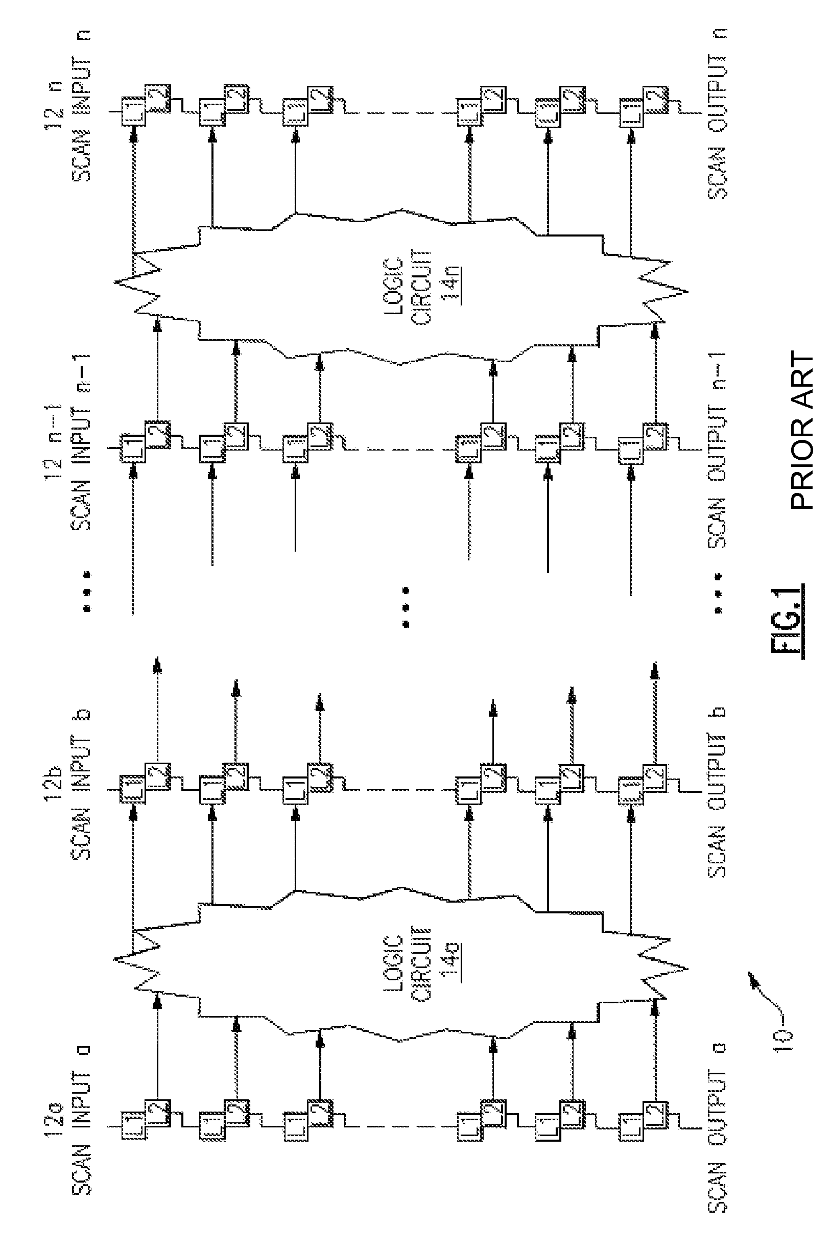
[0018]FIG. 1 is a schematic diagram of an example chip 10 which may be diagnosed with the present invention. The chip 10 is designed in a Level Sensitive Scan Design (LSSD), which includes scan chains 12a–12n which provide access to internal logic circuits 14a–14n in the chip 10. The scan chains 12 can be configured as one long chain or multiple short chains. As is known, data may be entered into a scan chain 12 at the input of the chain (WRPIN), and the data may be read at the output (WRPOUT) of the chain 12 to test the integrity of the chain, and to detect errors.

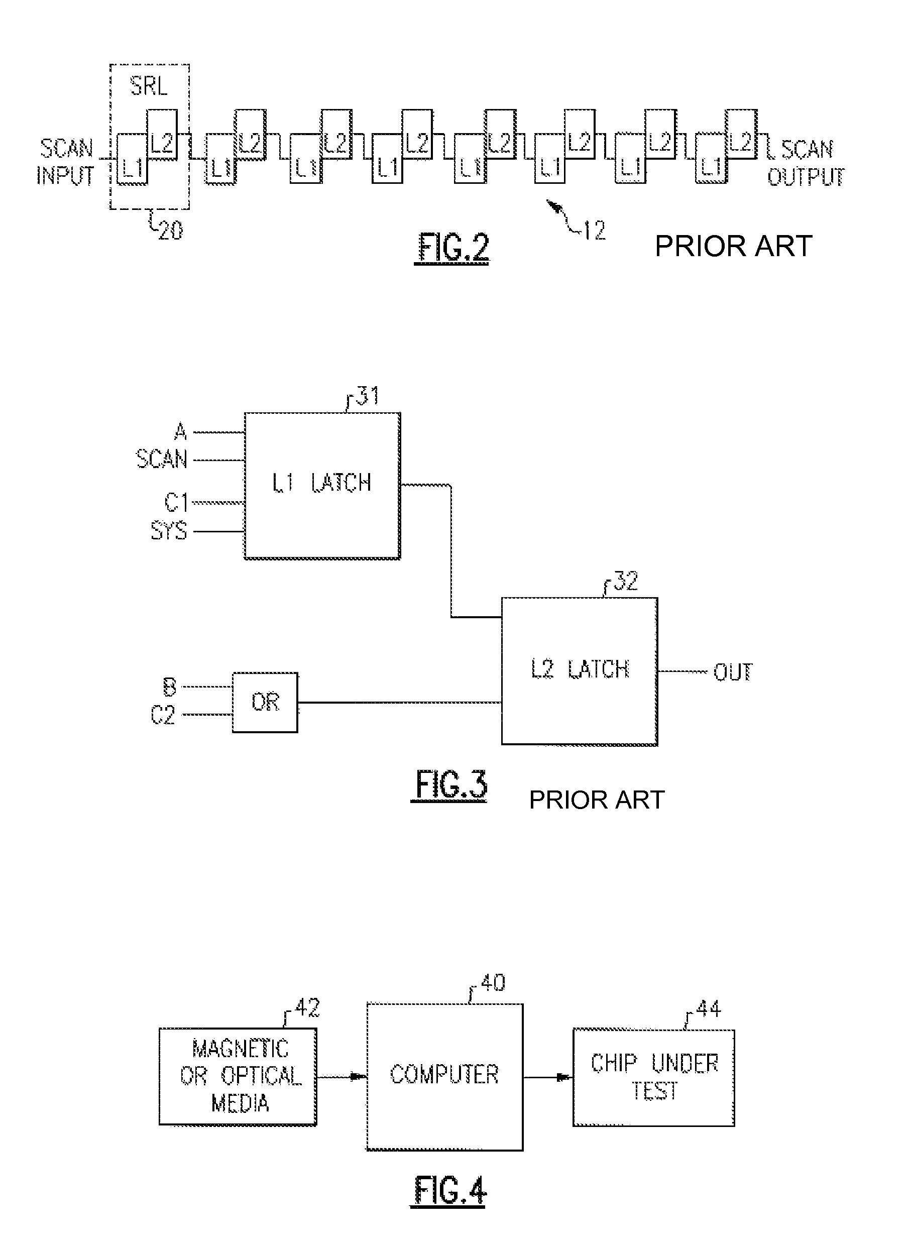
[0019]FIG. 2 is a schematic diagram of a scan chain 12 and is composed on a number of L1 / L2 shift register latch (SRL) pairs 20. As shown in FIG. 3, each SRL pair 20 consists of an L1 latch 31 connected to an L2 latch 32. When the A clock input of the L1 latch 31 is pulsed, the data at the SCAN port is captured and stored in the latch 31. Similarly, when the B or C2 clock inputs of the L2 latch is pulsed, the data from th...


PUM


Abstract

A method, apparatus and program product for testing at least one scan chain in an electronic chip in which the scan chain is formed by shift register latches arranged in the chain having a scan path with input pins and output pins. A flush test is executed for the scan chain under test and the flush test diagnostics for the flush test are recorded. A scan test is then executed for the scan chain under test and further test diagnostics are recorded in the event either or both the flush test or the scan test fails. The recorded flush test diagnostics and further test diagnostics are then analyzed to identify a call to one or more probable failed or failing shift register latches in the tested scan chain. The further scan chain diagnostics may include Disturb, Deterministic, ABIST, LBIST and Look-Ahead diagnostics. The tests may also be conducted for different voltage levels to determine the sensitivity of the scan chain being tested to differing voltage levels.

Description

FIELD OF THE INVENTION[0001]The present invention is related to a method and apparatus for testing and diagnosing scan chains in an electronic chip, and is more particularly related to a system and method for using algorithms for diagnosing scan chain failures.BACKGROUND OF THE INVENTION[0002]A number of different methods currently exist to diagnose scan chain failures in an electronic chip. See, for example, U.S. Pat. No. 3,761,695 issued Sep. 25, 1973 by Eichelberger for METHOD OF LEVEL SENSITIVE TESTING A FUNCTIONAL LOGIC SYSTEM; U.S. Pat. No. 6,308,290 B1 issued Oct. 23, 2001 to Forlenza et al. for LOOK AHEAD SCAN CHAIN DIAGNOSTIC METHOD; U.S. patent application US 2003 / 0131294 A1 published Jul. 10, 2003 by Motika et al. STUCK-AT FAULT SCAN CHAIN DIAGNOSTIC METHOD; U.S. patent Ser. No. 10 / 728,348 filed Dec. 4, 2003 by Forlenza et al. for ABIST-ASSISTED DETECTION OF SCAN CHAIN EFFECTS; U.S. patent application Ser. No. 10 / 767,046 filed Jan. 29, 2004 by Burdine for DIAGNOSTIC METHO...

Claims


Application Information

Patent Timeline
Patent Type & Authority Patents(United States)
IPC IPC(8): G01R31/28G06F17/50
CPCG01R31/318536G01R31/318569
Inventor BLASI, CHARLES J.BURDINE, TODD M.FORLENZA, ORAZIO P.
Owner GOOGLE LLC
Learn More