Light emitting diode

a light-emitting diode and diode technology, applied in semiconductor devices, semiconductor/solid-state device details, electrical devices, etc., can solve the problems of difficult to achieve the required light directivity control, the roughness height rating of the cup surface is limited, and the surface roughness height rating is less than or equal, etc., to achieve high heat resistance, high reflection effect, and high roughness height rating

Inactive Publication Date: 2007-07-03
CITIZEN ELECTRONICS CO LTD
View PDF3 Cites 35 Cited by
  • Summary
  • Abstract
  • Description
  • Claims
  • Application Information

AI Technical Summary

Benefits of technology

[0010]An object of the present invention is to provide a light emitting diode capable of producing light with a narrow directivity by improving functions of a reflection cup without using an additional member, such as a light collection member, as related art does.
[0013]The film body of this invention may be formed from, for example, a polyimide film by press forming. The polyimide film has advantages such as a very fine surface roughness height rating and a high heat resistance. The shape of the formed film body depends on the shapes of the male and female molds used for press forming.
[0014]In one example of this invention, the film body has its surface deposited with aluminum or silver, which has a high reflection effect. This metal deposition is generally done by evaporation. The surface roughness height rating of the deposited metal film is less than or equal to one-half the wavelength λ of light emitted from the light emitting element. With the surface roughness kept at less than or equal to one-half the wavelength λ, the diffusion of the reflected light can be decreased or minimized, easily producing light with a narrow directivity.
[0015]In another example of this invention, the light emitting element is flip-chip mounted on the electrodes of the base substrate through bumps such as solder bumps, gold bumps,and soon. This mounting method enables a size reduction of the reflection cup, which in turn leads to a narrow directivity. The opening formed in the bottom of the reflection cup through which the bumps are connected to the electrodes of the base substrate need only be large enough to accommodate the bumps. This makes it possible to secure a wide reflection surface below the light emitting element (bottom surface of the reflection cup), contributing to a more efficient extraction of upwardly reflected light.
[0016]In still another example of this invention, a frame to support the reflection cup may be arranged on the back side of the reflection cup. Supporting the reflection cup with the frame facilitates the handling of the light emitting diode. Further, by providing spaces in the frame on the back side of the reflection cup and installing electronic components in these spaces, a further reduction in size can be realized. The electronic components include, for example, Zener diode, capacitor and resistor, all used to prevent an accumulation of electrostatic charges in the light emitting diode.
[0017]With this invention the use of a film with a fine surface roughness height rating as the reflection cup of the light emitting diode renders the control of light directivity easy, thus making it possible to produce light with a narrow directivity using a simple construction without an additional light collecting member.

Problems solved by technology

However, with the conventional light emitting diode described above, since many of the reflection cups are resin-molded products, there is a limitation on the roughness height rating of their cup surfaces.
Even if the surface of the reflection cup is deposited or plated with a metal film, the surface roughness height rating which is less than or equal to one-half the wavelength λ of light emitted from the light emitting element, required for the control of light directivity is difficult to achieve.
Thus, the conventional reflection cup produces scattered rays of light, making it impossible to realize a desired narrow directivity with only the conventional reflection cup.
It has been therefore necessary to provide an additional member such as the light collecting member 6, rendering the device that much costly.
Other problems of the conventional device include a nonuniform color of emitted light due to chromatic aberration and an increased size of the light emitting diode.

Method used


Image

  • Light emitting diode
  • Light emitting diode
  • Light emitting diode

Examples


Embodiment Construction

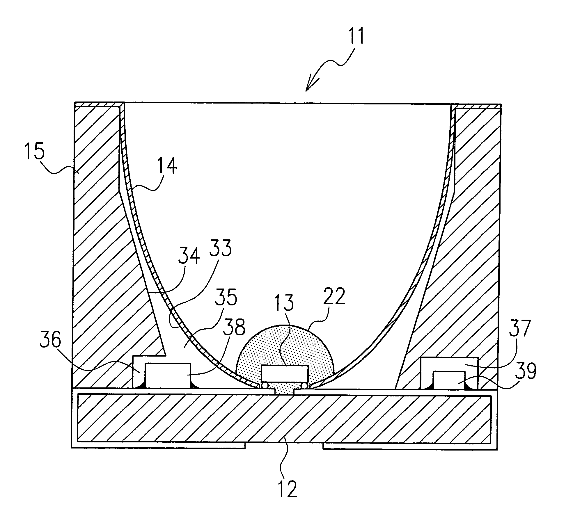
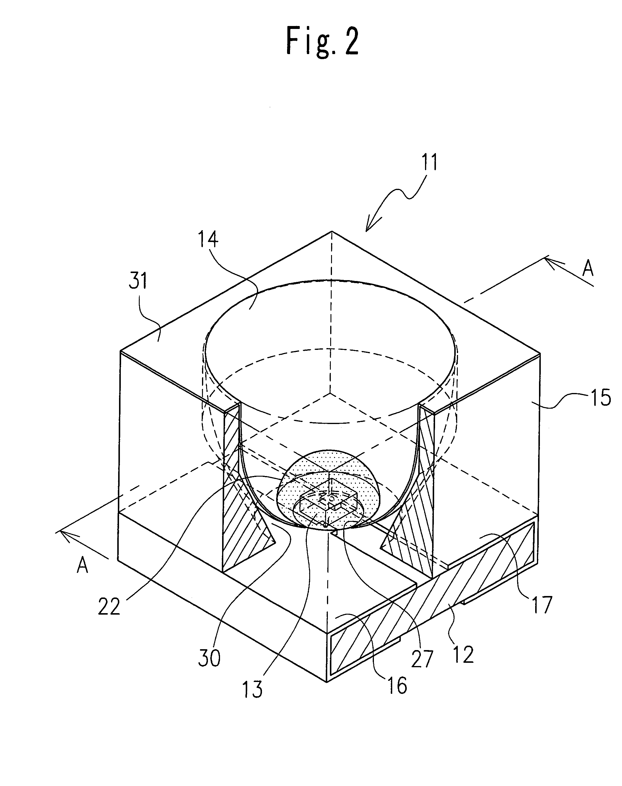
[0024]Now, embodiments of the light emitting diode of this invention will be described in detail by referring to the accompanying drawings. FIG. 2 is a perspective view showing an entire construction of the light emitting diode as one embodiment of this invention. FIG. 3 is a cross-sectional view taken along the line A—A of FIG. 2. FIG. 4 is an enlarged view of a part B of FIG. 3.

[0025]As shown in FIG. 2 to FIG. 4, a light emitting diode 11 of this invention has an almost square base substrate 12 having a pair of electrodes formed on a surface of a glass epoxy substrate, a light emitting element 13 arranged at an almost central part of an upper surface of the base substrate 12, a reflection cup 14 arranged to surround the light emitting element 13 to control a directivity of light emitted from the light emitting element 13, and a frame 15 arranged on a back side of the reflection cup 14 to support it.

[0026]The paired electrodes formed on the base substrate 12 are made up of a cathod...


PUM


Abstract

A light emitting diode comprising: a base substrate having a pair of electrodes; a reflection cup installed on the base substrate; a light emitting element arranged at a bottom of the reflection cup; and a resin sealant enclosing the light emitting element; wherein the light emitting element is electrically connected to the electrodes through an opening formed in the bottom of the reflection cup; wherein the reflection cup comprises a film body held in a cup shape and a metal film formed on a surface of the film body. This construction makes the control of light directivity easy and can produce light with a narrow directivity.

Description

CROSS REFERENCE TO RELATED APPLICATION[0001]The application claims the priority benefit of Japanese Patent Application No. 2003-340988, filed on Sep. 30, 2003, the entire description of which is incorporated herein by reference.BACKGROUND OF THE INVENTION[0002]1. Field of the Invention[0003]The present invention relates to a light emitting diode used for illuminating a variety of electronic devices and also in recent years for illuminating Panel meters of automobiles, and in particular, relates to a light emitting diode provided with a reflection cup to give an illuminating light a desired directivity.[0004]2. Description of Related Art[0005]An example of light emitting diode of this kind is disclosed in Japanese Patent Disclosure No. 2002-324917. This light emitting diode, as shown in FIG. 1, comprises a base substrate 2 surface-mounted on a mother board 1, a light emitting element 3 put on an upper surface of the base substrate 2, a reflection cup 4 arranged to surround the light ...

Claims


Application Information

Patent Timeline
Patent Type & Authority Patents(United States)
IPC IPC(8): H01L33/00H01L21/60H01L23/00H01L33/54H01L33/56H01L33/60
CPCH01L33/60H01L25/167H01L33/486H01L33/54H01L2224/48227H01L2924/01078H01L2924/01079H01L2924/19041H01L2924/01068H01L2924/12041
Inventor KUWABARA, YASUKIWAKATSUKI, TOSHIYUKI
Owner CITIZEN ELECTRONICS CO LTD
Why Eureka
Try Eureka