

Selectable inversion of differential input and/or output pins in programmable logic devices
a programmable logic and input/output pin technology, applied in logic circuit coupling/interface arrangement, pulse technique, instruments, etc., to achieve the effect of reverse the polarity of the differential signal
- Summary
- Abstract
- Description
- Claims
- Application Information
AI Technical Summary
Benefits of technology
Problems solved by technology
Method used
Image

Examples
Embodiment Construction
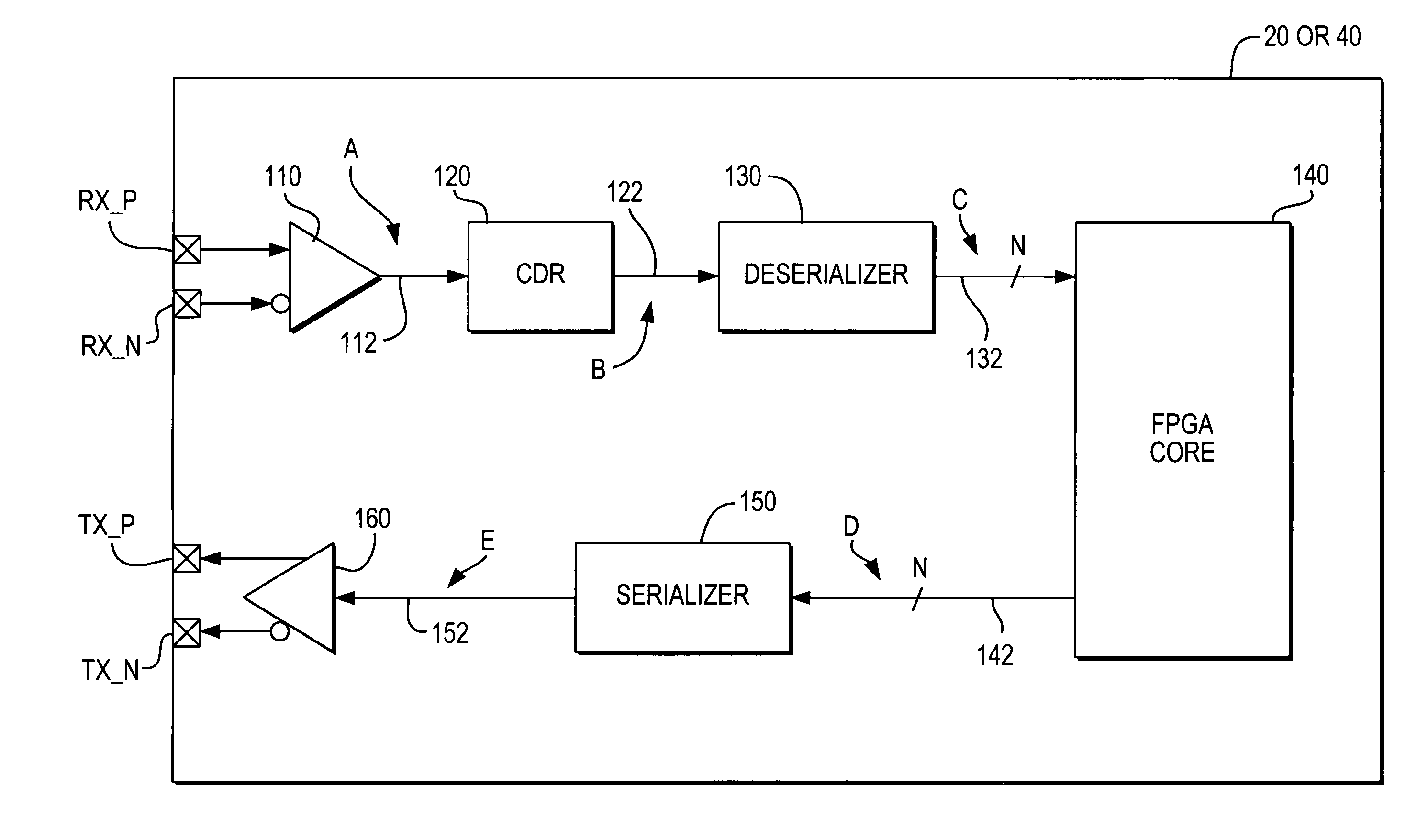
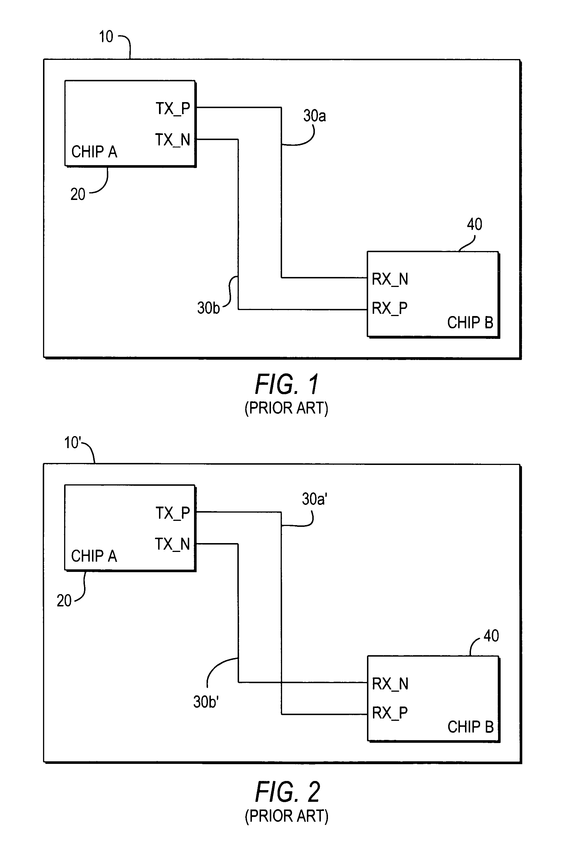
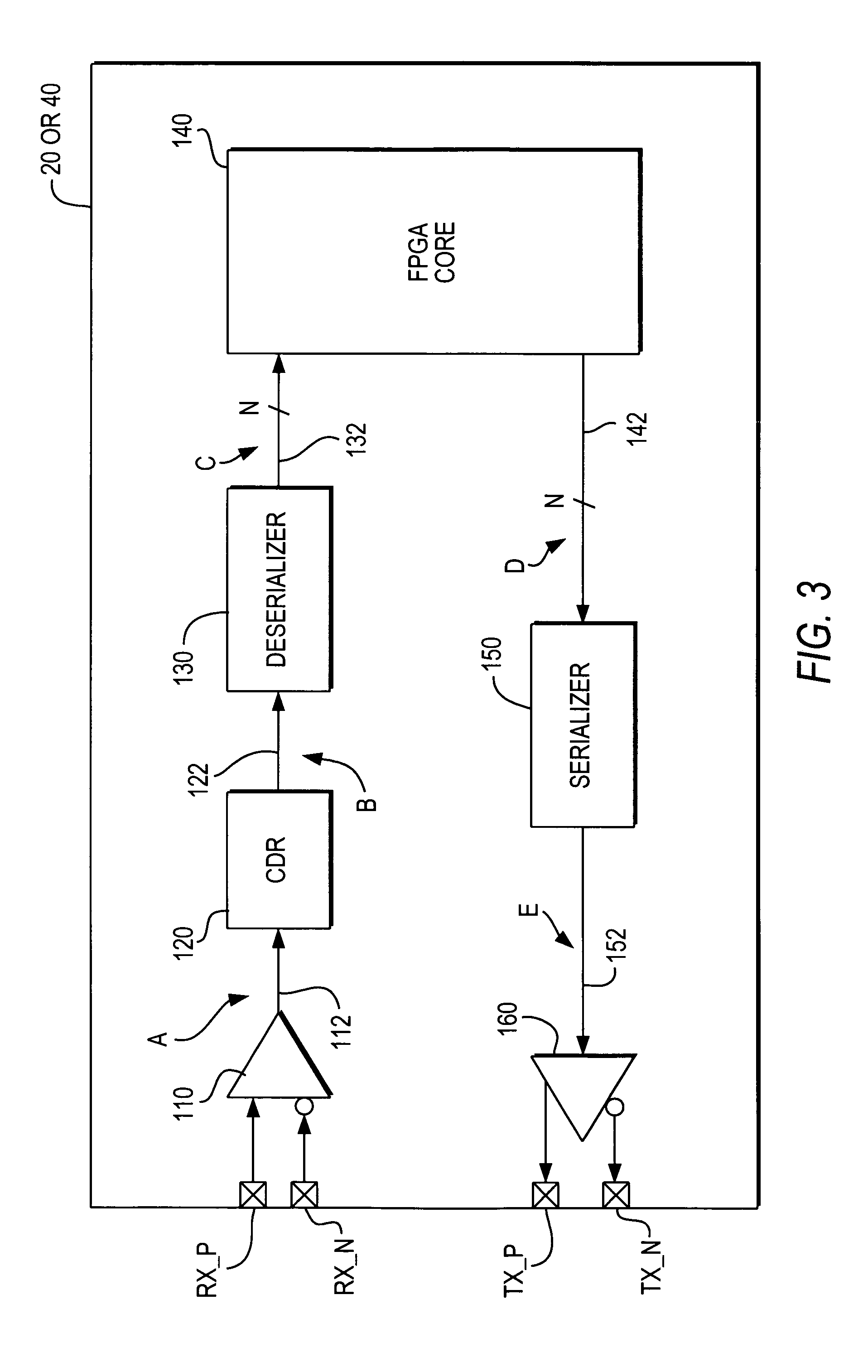
[0011]FIG. 1 shows an illustrative printed circuit board (“PCB”) 10 on which are mounted two integrated circuit devices 20 and 30 (also labeled “Chip A” and “Chip B”, respectively). PCB 20 has differential output pins TX_P and TX_N for outputting a pair of differential signals to a pair of PCB signal or circuit traces 30a and 30b on PCB 10. As is typical for differential signaling, this pair of signals actually represents only a single piece (e.g., bit) of information at any one time. For example, logic 1 may be represented by signal TX_P having a relatively high voltage or potential, concurrently with signal TX_N having a relatively low voltage or potential. Conversely, logic 0 may be represented by signal TX_N having a relatively high voltage or potential, concurrently with signal TX_P having a relatively low voltage or potential. As an alternative to potential differences as described in the two preceding sentences, the direction of current flow through pins TX_P and TX_N can be ...
PUM
 Abstract
Description
Claims
Application Information