Semiconductor device and method for manufacturing same

a semiconductor and semiconductor technology, applied in semiconductor devices, semiconductor/solid-state device details, electrical devices, etc., can solve the problems of high manufacturing cost, complicated system-on-chip manufacturing process, and large capital investment, and achieve the effect of increasing signal transmission speed

Inactive Publication Date: 2007-07-24
ACHLYS TECH INC
View PDF21 Cites 25 Cited by
  • Summary
  • Abstract
  • Description
  • Claims
  • Application Information

AI Technical Summary

Benefits of technology

[0012]It is a first object of the present invention to provide a semiconductor device which can increase signal transmission speed.

Problems solved by technology

However, the system-on-chip is complicated in manufacture process, requiring a huge amount of capital investment and hence high manufacture cost.
Consequently, signals could not be transmitted at sufficient high speed.
Meanwhile, even if the wiring length is tried to decrease throughout the entire semiconductor device, there is encountered a low freedom in design, e.g. restriction in semiconductor chip arrangement.

Method used


Image

  • Semiconductor device and method for manufacturing same
  • Semiconductor device and method for manufacturing same
  • Semiconductor device and method for manufacturing same

Examples


Embodiment Construction

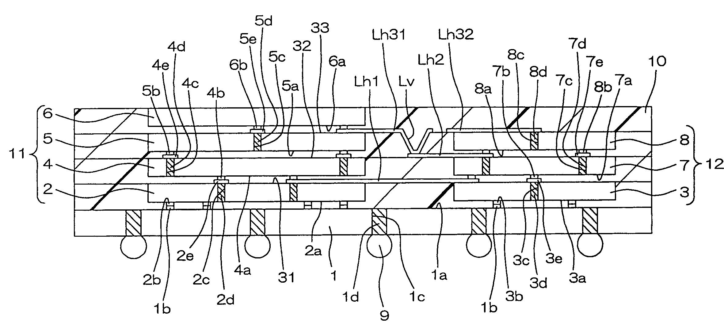
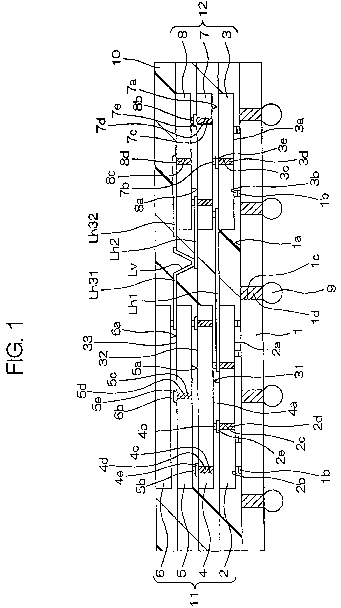
[0076]FIG. 1 is an illustrative sectional view showing a structure of a semiconductor device according an embodiment of the present invention.

[0077]A parent chip 1 is a semiconductor chip having external-connection electrodes (bumps 9), which is connected thereon with chip blocks 11, 12 each having a plurality of semiconductor chips (child chips) vertically superposed one upon another. Namely, the parent chip 1 serves as a support semiconductor chip to support the chip blocks 11, 12. The chip block 11 includes four child chips 2, 4, 5, 6 arranged one over another from a proximate end toward a distal end to the parent chip 1. The chip block 12 includes three child chips 3, 7, 8 arranged one over another from a proximate end toward a distal end to the parent chip 1. On the parent chip 1, polyimide resin 10 covers laterally the chip blocks 11, 12 and over the chip block 12. This structures the semiconductor device nearly in a cuboid form.

[0078]The parent chip 1, the child chip 2 and ch...


PUM


Abstract

There is provided a semiconductor device of a chip-on-chip structure having a support semiconductor chip, first and second chip blocks supported and connected on one surface of the support semiconductor chip and an insulator arranged between the first and second chip blocks. The first and second chip blocks each include one or a plurality of semiconductor chips having an active surface nearly parallel with the one surface of the support semiconductor chip. Within the insulator, an intralevel wiring is arranged on a wiring plane as a plane including an inactive or active surface of any of the semiconductor chips structuring the first or second chip block.

Description

[0001]This is a Divisional of U.S. application Ser. No.: 10 / 284,318, filed Oct. 31, 2002 now U.S. Pat. No. 6,867,501.BACKGROUND OF THE INVENTION[0002]1. Field of the Invention[0003]The present invention relates to a semiconductor device of a chip-on-chip structure that has a semiconductor chip bonded with other semiconductor chips thereon, and to a method for manufacturing same.[0004]2. Description of Related Art[0005]There are semiconductor devices increased in integration degree, including system-on-chips (SOCs) and multi-chip modules (MCMs). In the system-on-chip, the functions conventionally realized on a plurality of ICs are integrated on one semiconductor chip. Meanwhile, the multi-chip module is structured by a plurality of semiconductor chips arranged with density on a wiring board of glass-epoxy or the like. Each of them has multiple functions as one semiconductor device and can be size-reduced as compared to a combination of a plurality of semiconductor devices realizing t...

Claims


Application Information

Patent Timeline
Patent Type & Authority Patents(United States)
IPC IPC(8): H01L21/50H01L21/98H01L23/538H01L25/065
CPCH01L23/5389H01L24/24H01L24/82H01L25/0652H01L25/50H01L2224/24226H01L2225/06524H01L2225/06541H01L2924/01029H01L2924/01078H01L2924/15311H01L2924/01019H01L2924/01023H01L2924/01033H01L2924/014H01L2224/24137H01L2924/12042H01L2924/00
Inventor SHIBATA, KAZUTAKA
Owner ACHLYS TECH INC
Why Eureka
Try Eureka