Liquid crystal display panel with wide column spacers for keeping gap constant and process for fabrication thereof

a technology of liquid crystal display panel and column spacer, which is applied in the direction of non-linear optics, instruments, optics, etc., can solve the problems of increasing the gap along the lower edge of the display panel, and achieve the effect of reducing the surface tension between the liquid crystal and the orientation layer

Inactive Publication Date: 2007-07-24
NEC LCD TECH CORP
View PDF19 Cites 23 Cited by
  • Summary
  • Abstract
  • Description
  • Claims
  • Application Information

AI Technical Summary

Benefits of technology

[0021]It is also an important object of the present invention to provide a process for fabricating the liquid crystal display panel free from the partially whitened visual image.
[0022]The present inventor contemplated the problem inherent in the prior art liquid crystal display panel, and noticed that the partially whitened visual image was produced at high environmental temperature when the liquid crystal display panel was vertically placed on a surface. The present inventor measured the gap between the active matrix substrate structure and the counter substrate structure, and found that the gap was increased along the lower edge of the display panel. When the liquid crystal display panel was in a high environmental temperature, surface tension between the liquid crystal and the orientation layers was decreased, and tended to make a descent due to the gravity exerted thereon. This resulted in the increase of the gap along the lower edge of the display panel. The thick liquid crystal along the lower edge made the visual image partially whitened.

Problems solved by technology

This resulted in the increase of the gap along the lower edge of the display panel.

Method used


Image

  • Liquid crystal display panel with wide column spacers for keeping gap constant and process for fabrication thereof
  • Liquid crystal display panel with wide column spacers for keeping gap constant and process for fabrication thereof
  • Liquid crystal display panel with wide column spacers for keeping gap constant and process for fabrication thereof

Examples


first embodiment

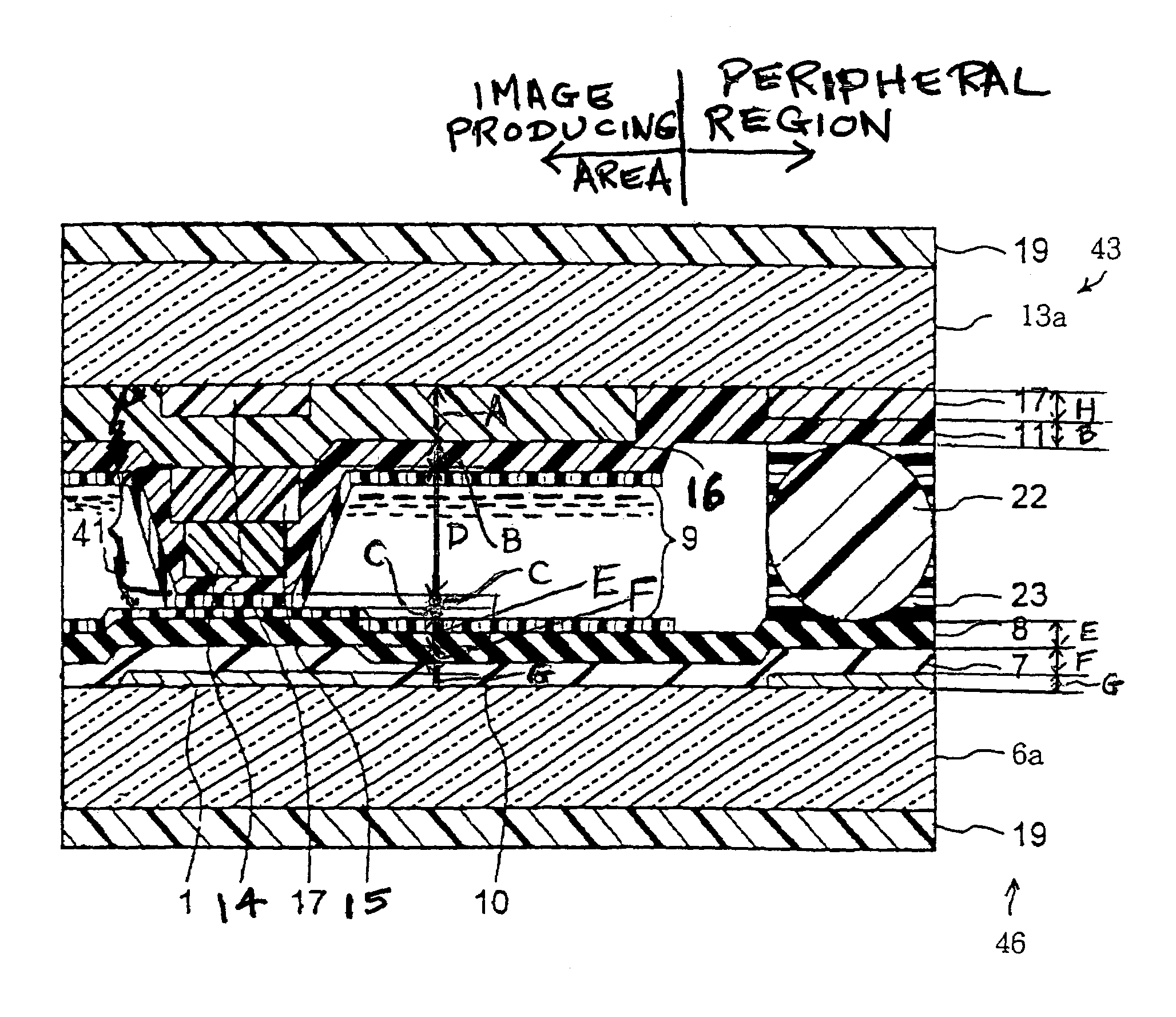
[0039]Referring to FIGS. 5, 6 and 7 of the drawings, an LPS liquid crystal display panel embodying the present invention largely comprises an active matrix substrate structure 46, a counter substrate structure 43, a sealing layer 23 and nematic liquid crystal 10. The active matrix substrate structure 46 is opposed to the counter substrate structure 43, and sealing layer 23 creates a gap between the active matrix substrate structure 46 and the counter substrate structure 43. The nematic liquid crystal 10 is injected through an inlet port 25 into the gap, and the gap between the active matrix substrate structure 46 and the counter substrate structure 43 is filled with the liquid crystal 10. Spherical spacers 22 reinforce the sealing resin layer 23, and column spacers 41 keep the gap between the active matrix substrate structure 46 and the counter substrate structure 43 constant. The nematic liquid crystal 10 has the positive anisotropic dielectric constant Δε of 7.0 and anisotropic re...

second embodiment

[0066]FIG. 9 illustrates a matrix of pixels R / G / B and column spacers 51 incorporated in another liquid crystal display panel. The IPS technology is employed in the liquid crystal display panel implementing the second embodiment. For this reason, the liquid crystal display panel implementing the second embodiment is similar in structure to the first embodiment except for the layout of the column spacers 51. The color filters 14 / 16 / 15 are respectively incorporated in the pixels R / G / B.

[0067]The pixels R / G / B are arranged in a matrix, and the column spacers 51 are located in the matrix. Each of the column spacers 51 is associated with plural pixels R / G / B. In this instance, each column spacers 51 is associated with six pixels R / G / B, and is provided at the boundary between the associated two pixels G. As a result, the column spacers 51 are checkerwise arranged. Although the contact area is widened, the ratio of total contact area to total pixel occupation area is fallen within the above-de...

third embodiment

[0070]Turning to FIG. 10 of the drawings, pixels R / G / B are arranged in matrix, and column spacers A / B are formed in the matrix of pixels R / G / B. The color filters 14 / 16 / 15 are respectively incorporated in the pixels R / G / B, and each of the column spacers A / B are formed at the boundary between adjacent two pixels G. The liquid crystal display panel implementing the third embodiment includes the active matrix substrate structure 46 and a counter substrate structure. The counter substrate structure is similar to the counter substrate structure 43 except the column spacers A / B.

[0071]Although the overcoat layer 11 and the orientation layer 9 are removed from the column spacers A / B, the column spacers A and B have a three-layered structure and a two-layered structure, respectively, as shown in figures 11A and 11B. The column spacers A / B are alternately arranged in the matrix of pixels R / G / B. The column spacers A are identical with the column spacers41, and are held in contact with the orien...


PUM

PropertyMeasurementUnit
diameteraaaaaaaaaa
pressureaaaaaaaaaa
anisotropic refractive index Δnaaaaaaaaaa

Abstract

An IPS (In-Plane-Switching) liquid crystal display panel has column spacers for spacing an active matrix substrate structure from a counter substrate structure, and liquid crystal fills the gap therebetween, wherein the ratio of total contact area between the column spacers and the active matrix substrate structure to the total area occupied by the pixels is fallen within the range from 0.050 percent to 0.150 percent so as to prevent the liquid crystal display panel from irregularity of brightness by keeping the gap constant.

Description

FIELD OF THE INVENTION[0001]This invention relates to a liquid crystal display panel and, more particularly, to a liquid crystal display panel having substrate structures spaced from one another by spacers and a process for fabricating the liquid crystal display panel.DESCRIPTION OF THE RELATED ART[0002]The liquid crystal display panel is light, thin and low in electric power consumption, and is used as terminals of various information systems as well as an image reproducing system. The liquid crystal display panel includes a pair of substrate structures and liquid crystal filling the gap between the substrate structures. Twisted nematic liquid crystal and super twisted nematic liquid crystal are typical examples of the liquid crystal available for the liquid crystal display panel. The liquid crystal molecules change the tilt angle depending upon the strength of electric field applied across the liquid crystal layer. The liquid crystal display panel is virtually divided into pixels,...

Claims


Application Information

Patent Timeline
Patent Type & Authority Patents(United States)
IPC IPC(8): G02F1/1339G02F1/1341G02F1/1343G02F1/13G02F1/1333
CPCG02F1/13394G02F1/134363G02F2001/133388G02F2001/13396G02F1/133388G02F1/13396G02F1/13
Inventor SHIBAHARA, HIDEO
Owner NEC LCD TECH CORP
Why Eureka
Try Eureka