Display device

a display device and active matrix technology, applied in the direction of discharge tube luminescnet screens, discharge tube/lamp details, electric discharge lamps, etc., can solve the problems of display unevenness, high voltage drop, and difficulty in fabricating high-definition display devices, and achieve high image quality and high image quality

Active Publication Date: 2007-07-31
SEMICON ENERGY LAB CO LTD
View PDF64 Cites 28 Cited by
  • Summary
  • Abstract
  • Description
  • Claims
  • Application Information

AI Technical Summary

Benefits of technology

[0030]According to the invention, a display device with high image quality and high-definition can be obtained in which display unevenness due to a voltage drop in a wiring is suppressed. In addition, a display devi

Problems solved by technology

When wiring length increases according to the increase in size of a display device, such problem as a voltage drop arises.
There is a problem in that a voltage applied to each EL element varies with place by generation of the voltage drop so that display unevenness is caused.
Thus it makes difficult to fabricate a display device with high-definition.
With the increase in size of a display device, particularly in an active matrix display

Method used


Image

  • Display device
  • Display device
  • Display device

Examples


embodiment mode 1

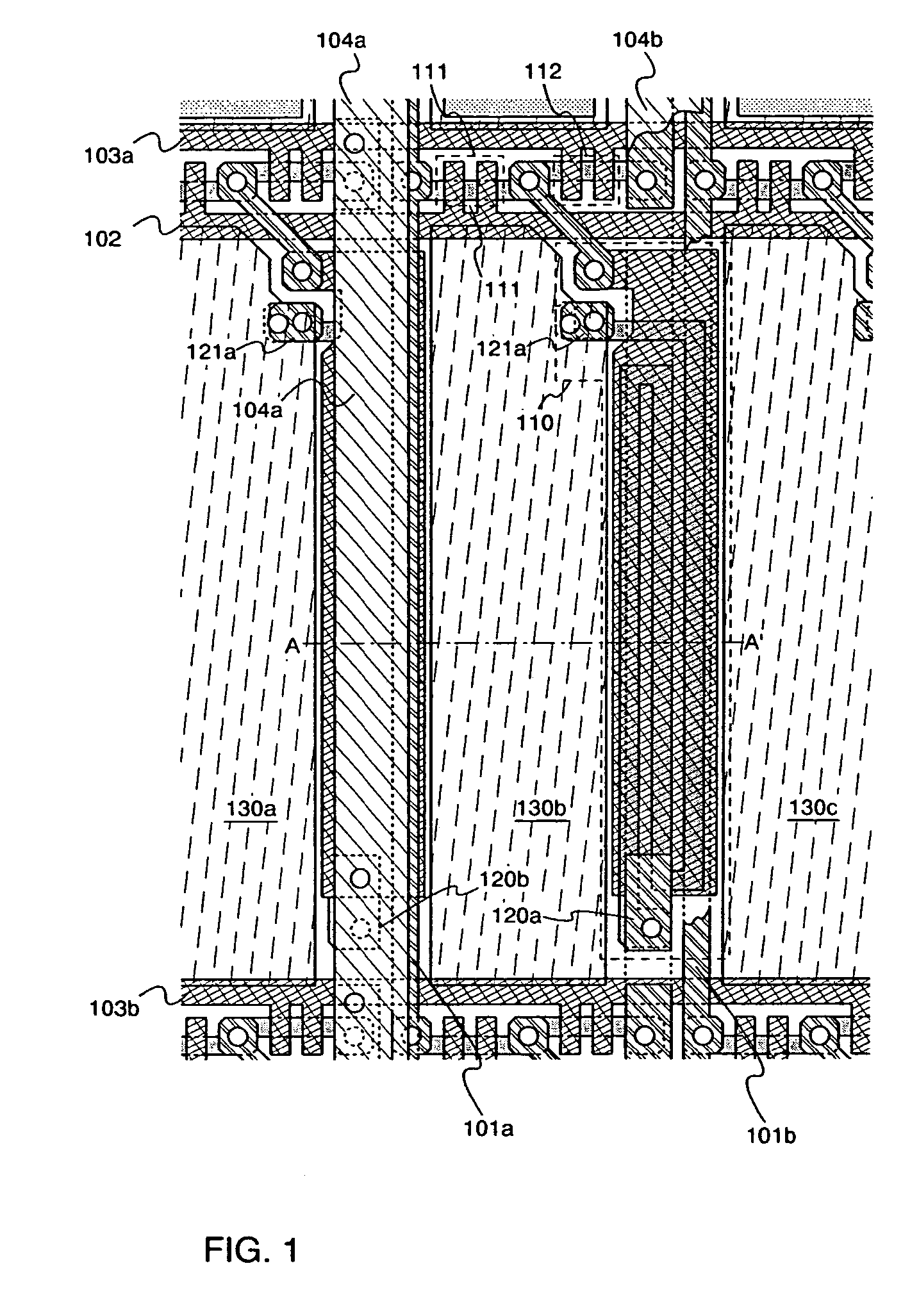
[0043]An embodiment mode of the invention will be explained with reference to FIG. 1.

[0044]FIG. 1 is a top plan view of a pixel portion of a display device to which the invention is applied. FIG. 9 is a cross-sectional view cutting along a line A–A′ of FIG. 1.

[0045]In FIG. 1, provided are a source signal line 101 (101a, 101b) as a wiring for transmitting a video signal and a current supply line 104 (104a, 104b) as a wiring for supplying a current to a light emitting element. The source signal line 101 and the current supply line 104 are formed on different layers with an insulating layer interposed therebetween to overlap with each other. In addition, they extend parallel to each other. Note that, although the entire source signal line 101 and the current supply line 104 are overlapped with each other in this embodiment mode, a part of the source signal line 101 and a part of the current supply line 104 may be overlapped. In any case, the width of the current supply line 104 can be ...

embodiment mode 2

[0052]An embodiment mode of the invention will be explained with reference to FIG. 3.

[0053]FIG. 3 is a top plan view of a pixel portion of a display device to which the invention is applied. FIG. 10 is a cross-sectional view cutting along a line A–A′ of FIG. 3.

[0054]In FIG. 3, a source signal line 301 (301a, 301b) as a wiring for transmitting a video signal and a current supply line 305 (305a, 305b) as a wiring for supplying a current to a light emitting element are provided. The source signal line 301 and the current supply line 305 are formed on the same layer and extend parallel to each other. In addition, above the source signal line 301 and the current supply line 305, a wiring 304 is formed with an insulating layer interposed therebetween. The wiring 304 extends parallel to the source signal line 301 or the current supply line 305. The wiring 304 and the current supply line 305 are connected to each other through a contact hole. Note that, in this embodiment mode, a part of th...

embodiment mode 3

[0061]In each of the display devices shown in Embodiment Mode 1 and Embodiment Mode 2, the current supply line 104 or the wiring 305 are provided on the same layer as the first electrode 130 or 330 of the light emitting element respectively.

[0062]However, the structure of the display device of the invention is not limited to this, the first electrode 130 or 330 of the light emitting element may be provided over the current supply line 104 or the wiring 305 respectively with an insulating layer interposed therebetween. With such a structure, particularly in a display device of a upper surface emitting type, the opening part can be designed with more flexibility and the aperture ratio is improved.

[0063]In addition, in the fabricating process of a display device, a flattening process after the formation of a transparent conductive layer for forming the first electrodes 130 and 330 of the light emitting element may be simplified.


PUM


Abstract

A display device with high-definition, in which display unevenness due to a voltage drop in a wiring or display unevenness due to a variation in characteristics of TFTs are suppressed. The display device of the invention comprises a first wiring for transmitting a video signal and a second wiring for supplying a current to a light emitting element. The first wiring and the second wiring extend parallel to each other, and are formed so as to overlap with each other at least partly with an insulating layer interposed therebetween.

Description

BACKGROUND OF THE INVENTION[0001]1. Field of the Invention[0002]The present invention relates to an active matrix display device, and more particularly to a wiring structure of an active matrix display device comprising a light emitting element.[0003]2. Description of the Related Art[0004]In recent years, development of large-scale electroluminescence (hereinafter-abbreviated to EL) display device has been advanced with the intention of coming to the television market.[0005]When wiring length increases according to the increase in size of a display device, such problem as a voltage drop arises. There is a problem in that a voltage applied to each EL element varies with place by generation of the voltage drop so that display unevenness is caused.[0006]In the case where film thickness of the wiring is increased in order to solve the above-mentioned problem, a lot of loads are applied to the steps of forming film, etching and the like. In addition, in the case where line width of the w...

Claims


Application Information

Patent Timeline
IPC IPC(8): H05B33/00H01L27/12H01L27/32
CPCH01L27/12H01L27/3276H10K59/131
Inventor SAKAKURA, MASAYUKINAGAO, RITSUKOOSAME, MITSUAKIANZAI, AYAYAMAZAKI, YUTANADA, YOSHIFUMI
Owner SEMICON ENERGY LAB CO LTD
Why Eureka
Try Eureka