Method to reduce CD non-uniformity in IC manufacturing

Active Publication Date: 2007-08-07
TAIWAN SEMICON MFG CO LTD
View PDF10 Cites 199 Cited by
  • Summary
  • Abstract
  • Description
  • Claims
  • Application Information

AI Technical Summary

Benefits of technology

[0015]Another objective of the invention is to narrow the range of the distribution of the line-to-space ratio in a given mask pattern that is used for photolithographic exposure.
[0016]A method is provided for reducing Critical Dimension (CD) non-uniformity in creating a patterned layer of semiconductor material. A substrate is provided with one or more layers of semiconductor material, a first masking layer is deposited over the one or more layers of semiconductor material. A first pattern, comprising high-density semiconductor device features, isolated semiconductor device features and dummy features, is created in the first masking layer, thereby applying methods for compensation of optical proximity effects and micro-loading. The first pattern is transposed to at least one layer of the one o

Problems solved by technology

This method is therefore limited by t

Method used


Image

  • Method to reduce CD non-uniformity in IC manufacturing
  • Method to reduce CD non-uniformity in IC manufacturing
  • Method to reduce CD non-uniformity in IC manufacturing

Examples


Embodiment Construction

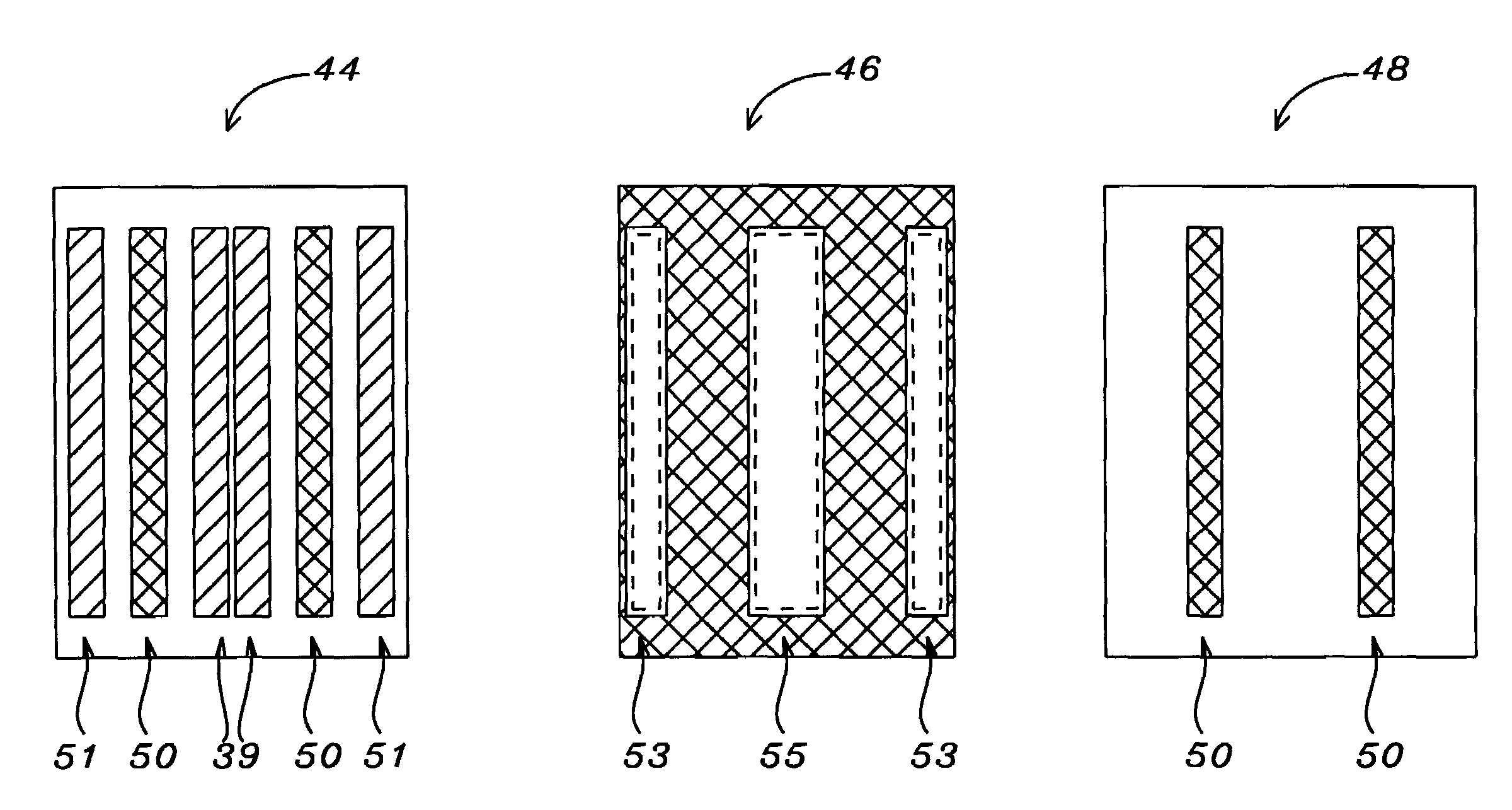
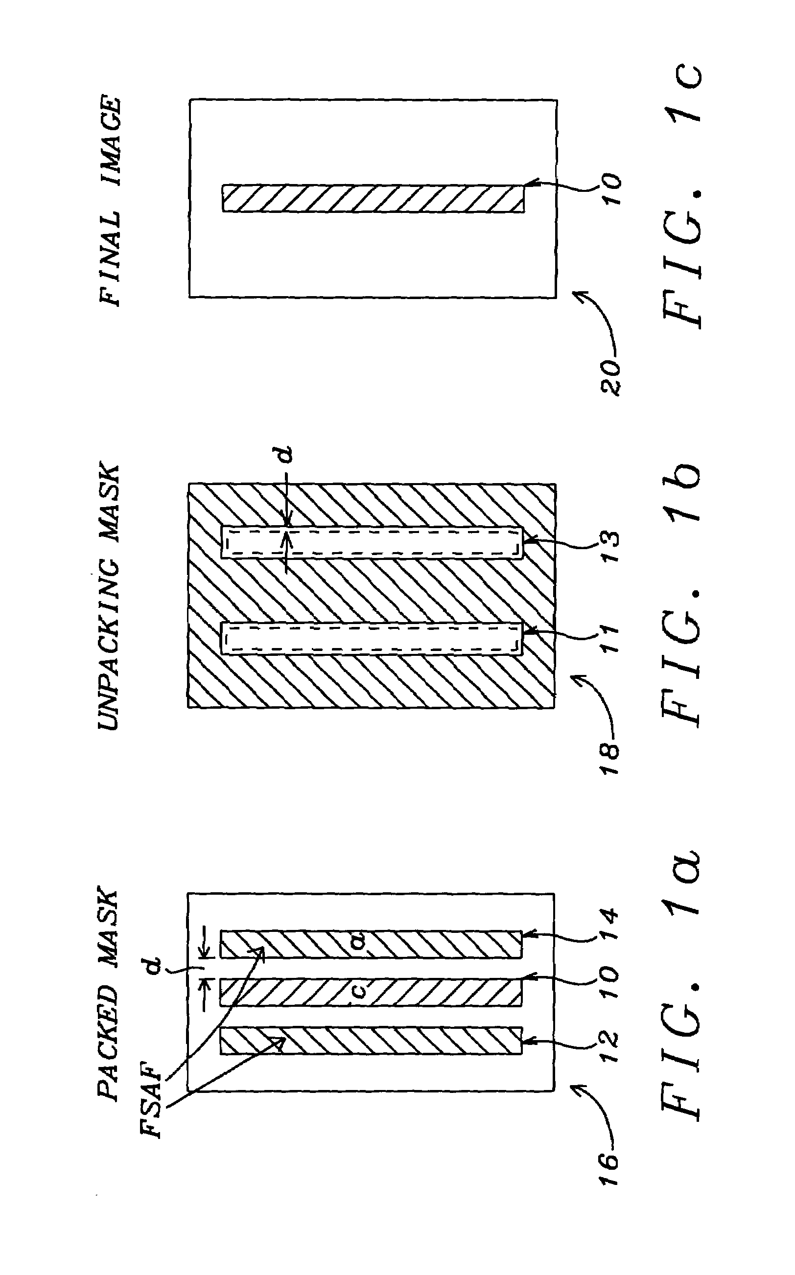
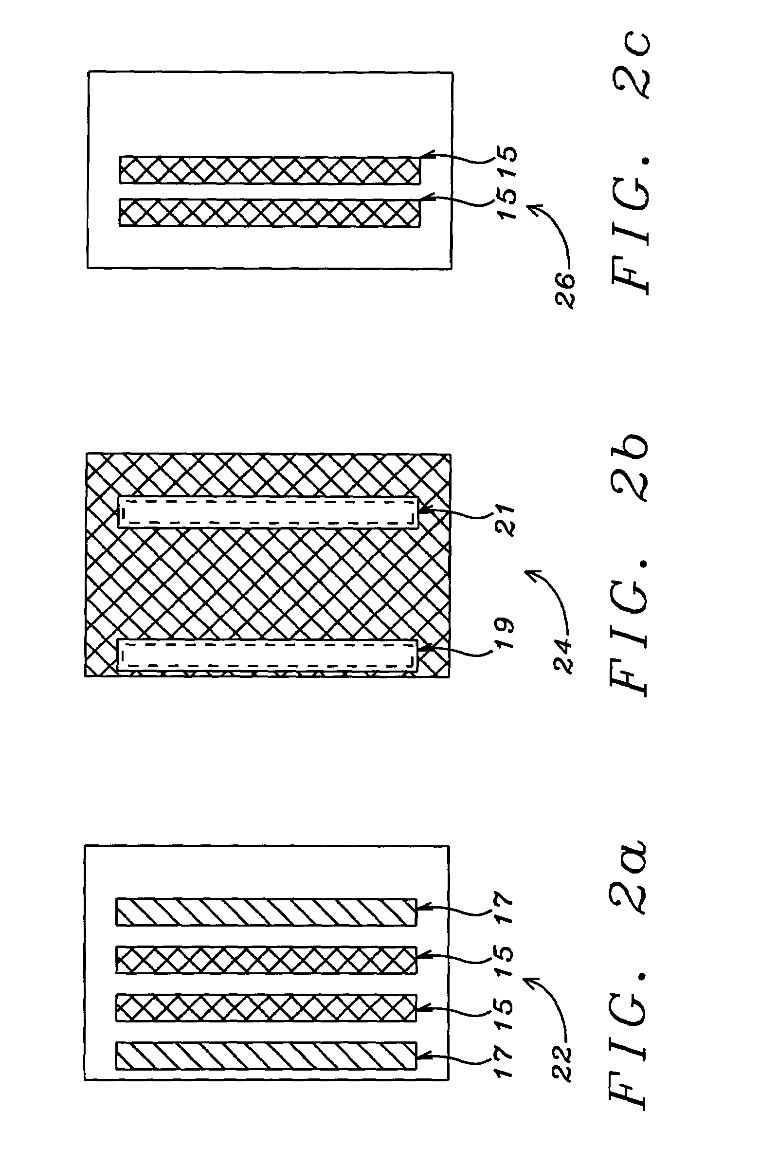
[0038]As has been previously highlighted, close line spacing in the range of a line-width to line-spacing (L / S) ratio of 1:1 are difficult to achieve for devices having resolution-limiting size, resulting in a narrow latitude of exposure and a small depth of focus or both. To correct this problem, a well-known method is to use off-axis illumination, in the form of annular, quadruple of dipole configurations. A limitation of this method is that the location of the ring, quadruples or dipoles can be optimized only for a special frequency in the object. For example, only the image of pairs of 1:1 spaced lines (line-width to line-spacing ratio) can be optimized. In this case of optimization, lines with a L:S=1:2 ratio will benefit less from this optimization scheme, lines that are spaced further apart benefit even less. This scheme can be applied to lines with for instance L:S=1:2 but this optimization is achieved at the expense of lines with higher and lower ratios of L:S.

[0039]A frequ...


PUM


Abstract

A method is provided for reducing Critical Dimension (CD) non-uniformity in creating a patterned layer of semiconductor material. Two masking layers are respectively created, the first masking layer comprising a main pattern, an isolated pattern and a dummy pattern, the second masking layer exposing the dummy pattern. Methods of compensating for optical proximity effects and micro-loading, as provided by the invention, are applied in creating the first masking layer. The patterned first masking layer is transposed to an underlying layer creating a first pattern therein. The second masking layer removes the dummy features from the transposed first pattern, creating a second pattern therein comprising a main pattern and an isolated pattern to which compensation for optical proximity effects and micro-loading have been applied. The second pattern serves for additional etching of underlying semiconductor material.

Description

[0001]This application is a continuation-in-part of Ser. No. 10 / 125,215 filing date Apr. 18, 2002 now U.S. Pat. No. 6,929,887, assigned to common assignee.BACKGROUND OF THE INVENTION[0002](1) Field of the Invention[0003]The invention relates to the fabrication of integrated circuit devices, and more particularly, to a method to further improve the imaging of patterns that are used in photolithography by providing improved enhancement effects for sub-resolution lines that are added to a line pattern, to address issues of having insufficient space in order to add sub-resolution lines and issues of avoiding printing sub-resolution lines.[0004](2) Description of the Prior Art[0005]The creation of semiconductor devices requires numerous interacting and mutually supporting disciplines. Addressed at this time are the disciplines that are required to create patterns on a semiconductor surface, such as the surface of a layer of photoresist or the surface of a semiconductor substrate.[0006]De...

Claims


Application Information

Patent Timeline
IPC IPC(8): G03F1/00G03F7/20
CPCG03F7/70433G03F7/70441
Inventor SHIN, JAW-JUNGKE, CHIH-MINGLIN, BURN-JENG
Owner TAIWAN SEMICON MFG CO LTD
Why Eureka
Try Eureka