Method for forming a finely patterned resist

Inactive Publication Date: 2006-07-13
TAIWAN SEMICON MFG CO LTD
View PDF3 Cites 153 Cited by
  • Summary
  • Abstract
  • Description
  • Claims
  • Application Information

AI Technical Summary

Benefits of technology

[0009] To achieve the foregoing and other objects, and in accordance with the purposes of the present invention, as embodied and broadly desc

Problems solved by technology

One of the limiting factors in the continuing evolution toward smaller device semiconductor feature size and higher density has been the stringent requirements placed on photolithographic processes as line width and step heights have decreased.
For example, if the exposed resist region does not become fully soluble, resist profiles are compromised.
Proposed methods have included dry etching or trimming the resist following development, a method which is increasingly limited due

Method used


Image

  • Method for forming a finely patterned resist
  • Method for forming a finely patterned resist
  • Method for forming a finely patterned resist

Examples


Example

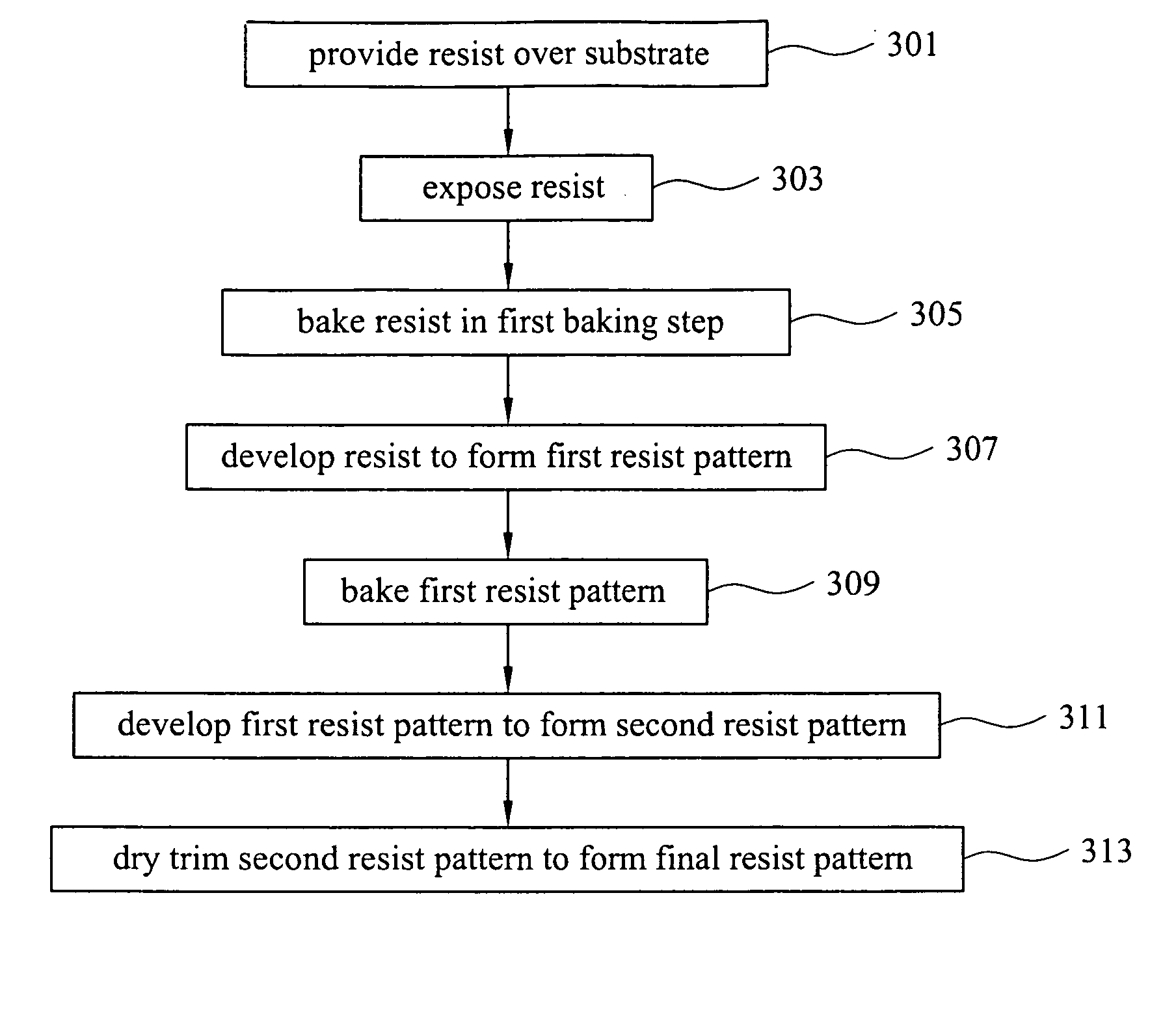
[0015] Although the present invention is explained with respect to, and particularly advantageous for, the formation of conductive interconnect lines in a multi-level integrated circuit semiconductor device, the method of the present invention may be used to achieve reduced CD sizes, for example, less than the wavelength of the exposing (illuminating) light in a lithographic process, for any type of resist pattern having an elongated shape, e.g., lines where a width portion is less than a length portion.

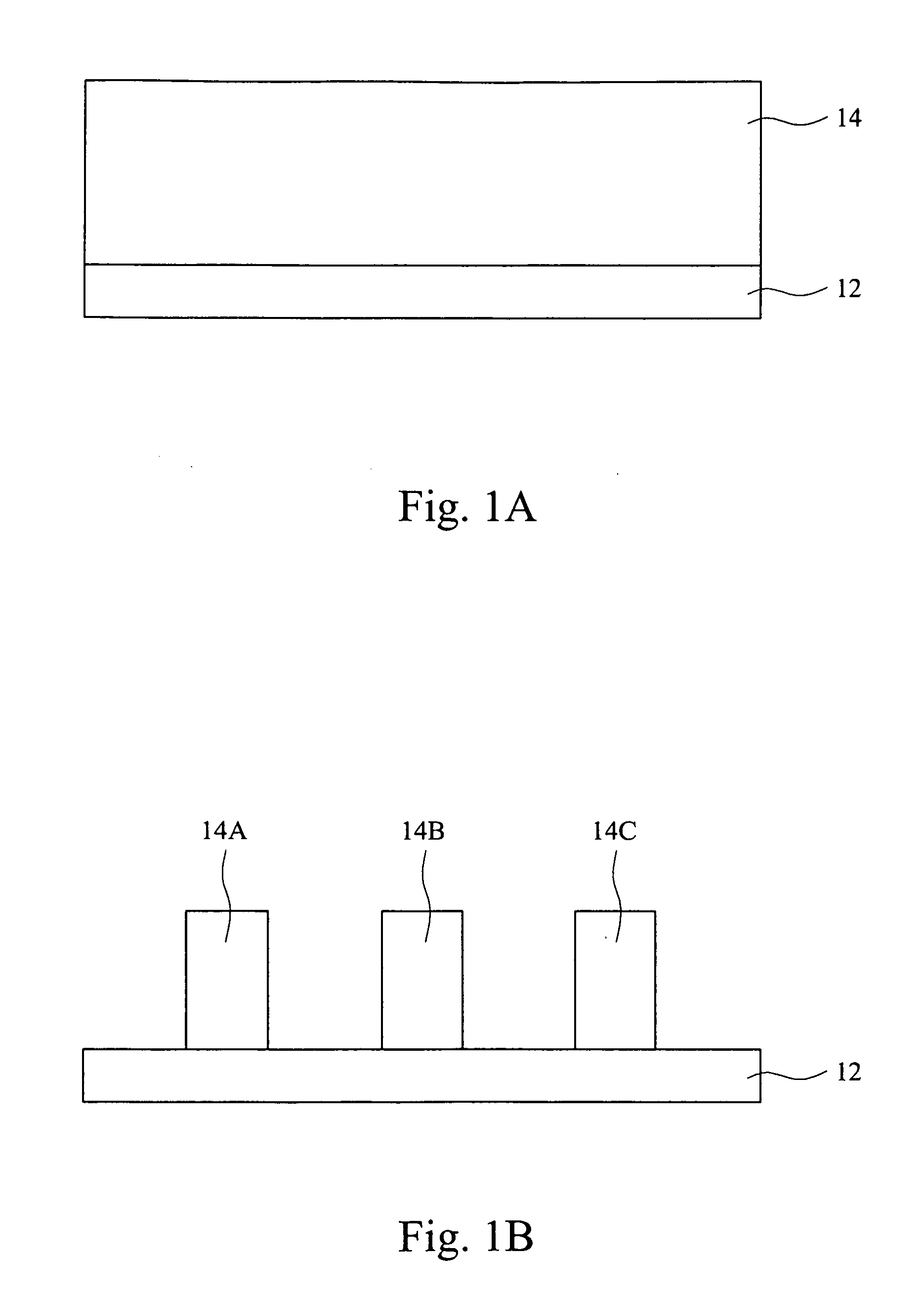
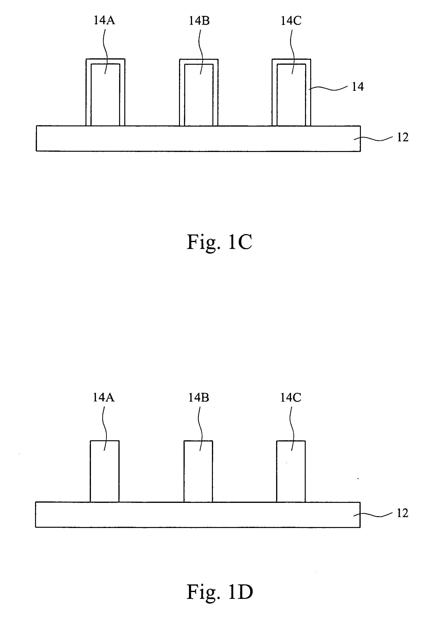
[0016] Referring to FIG. 1A is shown a portion of resist layer 14 overlying a portion of a substrate 12. It will be appreciated that the substrate may be any type of substrate including a dielectric insulating layer or a conductive layer for forming an elongated (e.g., line) pattern therein, e.g., damascene interconnect lines. Photoresist layer 14, in an important aspect of the invention is preferably a chemically amplified (CA) photoresist including a photoacid generator (PAG) acid...


PUM


Abstract

A method for reducing a critical dimension of a photoresist pattern while improving a line spacing between distal end portions of pattern lines wherein the method includes providing a substrate including an overlying resist; exposing the resist to an activating light source; baking the resist in a first baking process followed by developing the resist in a first development process to form a first resist pattern; then baking the first resist pattern in a second baking process followed by developing the first resist pattern in a second development process to form a second resist pattern having reduced dimensions; and, then dry trimming the second resist pattern to form a final resist pattern with reduced dimensions compared to the second resist pattern.

Description

FIELD OF THE INVENTION [0001] This invention generally relates to resist patterning techniques in integrated circuit semiconductor device manufacturing processes and more particularly to an improved method for producing a finely patterned resist layer including improved control over critical dimensions (CD's) while improving pattern feature spacing and improving a process flow. BACKGROUND OF THE INVENTION [0002] One of the limiting factors in the continuing evolution toward smaller device semiconductor feature size and higher density has been the stringent requirements placed on photolithographic processes as line width and step heights have decreased. Various resist trimming method methods have been proposed in prior art processes to achieve more finely dimension patterns following a resist exposure and development process. 003 For example, several different process variables may contribute to unacceptable resist profiles. Typically a photoresist layer is applied to a semiconductor...

Claims


Application Information

Patent Timeline
IPC IPC(8): G03F7/40
CPCG03F7/40
Inventor HO, BANG-CHEINCHEN, JIAN-HONG
Owner TAIWAN SEMICON MFG CO LTD
Why Eureka
Try Eureka