Method of fabricating a high-voltage transistor with an extended drain structure
What is AI technical title?
AI technical title is built by Patsnap AI team. It summarizes the technical point description of the patent document.
a high-voltage transistor and drain structure technology, applied in the field of semiconductor transistor structures with extended drain structures, can solve the problems of increasing on-state resistance, affecting the on-state performance of the device, and unsatisfactory need for a high-voltage transistor structure that can support still higher voltages
Inactive Publication Date: 2007-08-07
POWER INTEGRATIONS INC
View PDF140 Cites 67 Cited by
Summary
Abstract
Description
Claims
Application Information
AI Technical Summary
This helps you quickly interpret patents by identifying the three key elements:
Problems solved by technology
Method used
Benefits of technology
Problems solved by technology
The combined decrease in doping and increase in length of the extended drain region therefore have the deleterious effect on the on-state performance of the device, as both cause an increase in on-state resistance.
Although the device structures described above achieve high Vbd with relatively low on-state resistance as compared to earlier designs, there is still an unsatisfied need for a high-voltage transistor structure that can support still higher voltages while achieving a much lower on-state resistance.
Method used
Image
Click on the blue label to locate the original text in one second.
Reading with bidirectional positioning of images and text.
Examples
Embodiment Construction
[0018]A high-voltage field-effect transistor having an extended drain region and a method for making the same is described. The HVFET has a low specific on-state resistance and supports high voltage in the off-state. In the following description, numerous specific details are set forth, such as material types, doping levels, structural features, processing steps, etc., in order to provide a thorough understanding of the present invention. Practitioners having ordinary skill in the semiconductor arts will understand that the invention may be practiced without many of these details. In other instances, well-known elements, techniques, and processing steps have not been described in detail to avoid obscuring the invention.
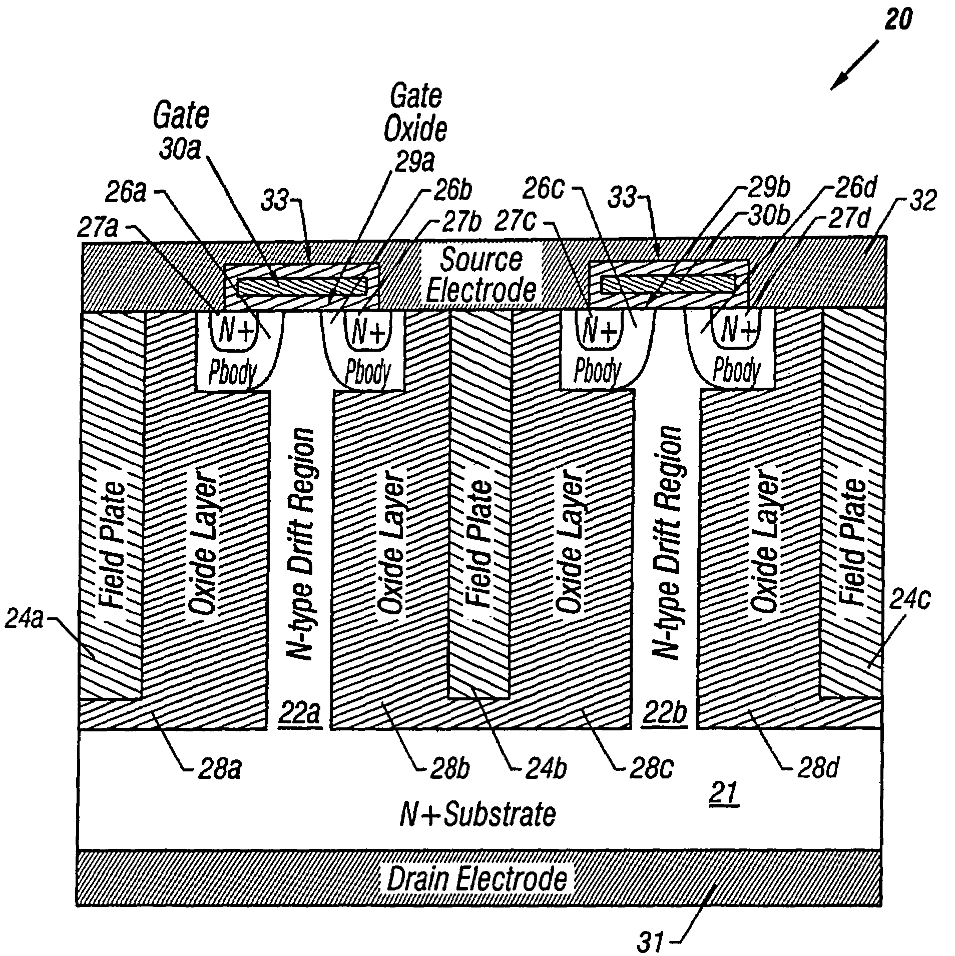
[0019]FIG. 1 is a cross-sectional side view of a vertical n-channel (i.e., NMOS) HVFET 20 in accordance with one embodiment of the present invention. It should be understood that the elements in the figures are representational, and are not drawn to scale in the inter...
PUM
Abstract
A method for fabricating a high-voltage transistor with an extended drain region includes forming in a semiconductor substrate of a first conductivity type, first and second trenches that define a mesa having respective first and second sidewalls; then partially filling each of the trenches with a dielectric material that covers the first and second sidewalls. The remaining portions of the trenches are then filled with a conductive material to form first and second field plates. Source and body regions are formed in an upper portion of the mesa, with the body region separating the source from a lower portion of the mesa. It is emphasized that this abstract is provided to comply with the rules requiring an abstract that will allow a searcher or other reader to quickly ascertain the subject matter of the technical disclosure. It is submitted with the understanding that it will not be used to interpret or limit the scope or meaning of the claims.
Description
RELATED APPLICATIONS[0001]This application is a continuation of application Ser. No. 10 / 722,792 filed Nov. 25, 2003, now U.S. Pat. No. 6,838,346 which is a continuation of application Ser. No. 10 / 278,551 filed Oct. 22, 2002, now U.S. Pat. No. 6,750,105, which is a division of application Ser. No. 09 / 948,879 filed Sep. 7, 2001, now U.S. Pat. No. 6,635,544, and is also related to application Ser. No. 10 / 278,432 filed Oct. 22, 2002, now U.S. Pat. No. 6,667,213, which applications are assigned to the assignee of the present application.FIELD OF THE INVENTION[0002]The present invention relates to semiconductor devices fabricated in a silicon substrate. More specifically, the present invention relates to field-effect semiconductor transistor structures capable of withstanding high voltages.BACKGROUND OF THE INVENTION[0003]High-voltage, field-effect transistors (HVFETs) are well known in the semiconductor arts. Most often, HVFETs comprise a device structure that includes an extended drain ...
Claims
Application Information
Patent Timeline
Application Date:The date an application was filed.
Publication Date:The date a patent or application was officially published.
First Publication Date:The earliest publication date of a patent with the same application number.
Issue Date:Publication date of the patent grant document.
PCT Entry Date:The Entry date of PCT National Phase.
Estimated Expiry Date:The statutory expiry date of a patent right according to the Patent Law, and it is the longest term of protection that the patent right can achieve without the termination of the patent right due to other reasons(Term extension factor has been taken into account ).
Invalid Date:Actual expiry date is based on effective date or publication date of legal transaction data of invalid patent.

