High-voltage MEMS apparatus and method

a high-voltage mems and apparatus technology, applied in the field of mems devices, can solve the problems of high-voltage biasing use that is not without complications, high-voltage devices and isolation regions may not be available in the lowest-cost semiconductor technology, and more expensive technologies. achieve the effect of reducing process cost and complexity

Active Publication Date: 2012-09-27
INVENSENSE
View PDF5 Cites 35 Cited by
  • Summary
  • Abstract
  • Description
  • Claims
  • Application Information

AI Technical Summary

Benefits of technology

[0006]A high-voltage MEMS system compatible with low-voltage semiconductor process technology is disclosed. The system comprises a MEMS device coupled to a high-voltage bias generator employing an extended-voltage isolation residing in a semiconductor technology substrate. The system avoids the use of high-voltage transistors so that special high-voltage processing steps are not required of the semiconductor technology, thereby reducing process cost and complexity. MEMS testing capability is addressed with a self-test circuit allowing modulation of the bias voltage and current so that a need for external high-voltage connections and associated electro-static discharge protection circuitry are also avoided.

Problems solved by technology

However, the use of high-voltage biasing is not without complications.
Such high-voltage devices and isolation regions may not be available in the lowest-cost semiconductor technologies which are typically low-voltage technologies, necessitating the use of more expensive technologies to enable high-voltage biasing and signal processing.
The performance gains afforded by the use of high-voltage may therefore be contrary to the goal of cost reduction.

Method used


Image

  • High-voltage MEMS apparatus and method
  • High-voltage MEMS apparatus and method
  • High-voltage MEMS apparatus and method

Examples


Embodiment Construction

[0017]The present invention relates generally to MEMS devices and specifically to a method and system for utilizing a MEMS device in a high voltage environment. The following description is presented to enable one of ordinary skill in the art to make and use the invention and is provided in the context of a patent application and its requirements. Various modifications to the preferred embodiments and the generic principles and features described herein will be readily apparent to those skilled in the art. Thus, the present invention is not intended to be limited to the embodiments shown, but is to be accorded the widest scope consistent with the principles and features described herein.

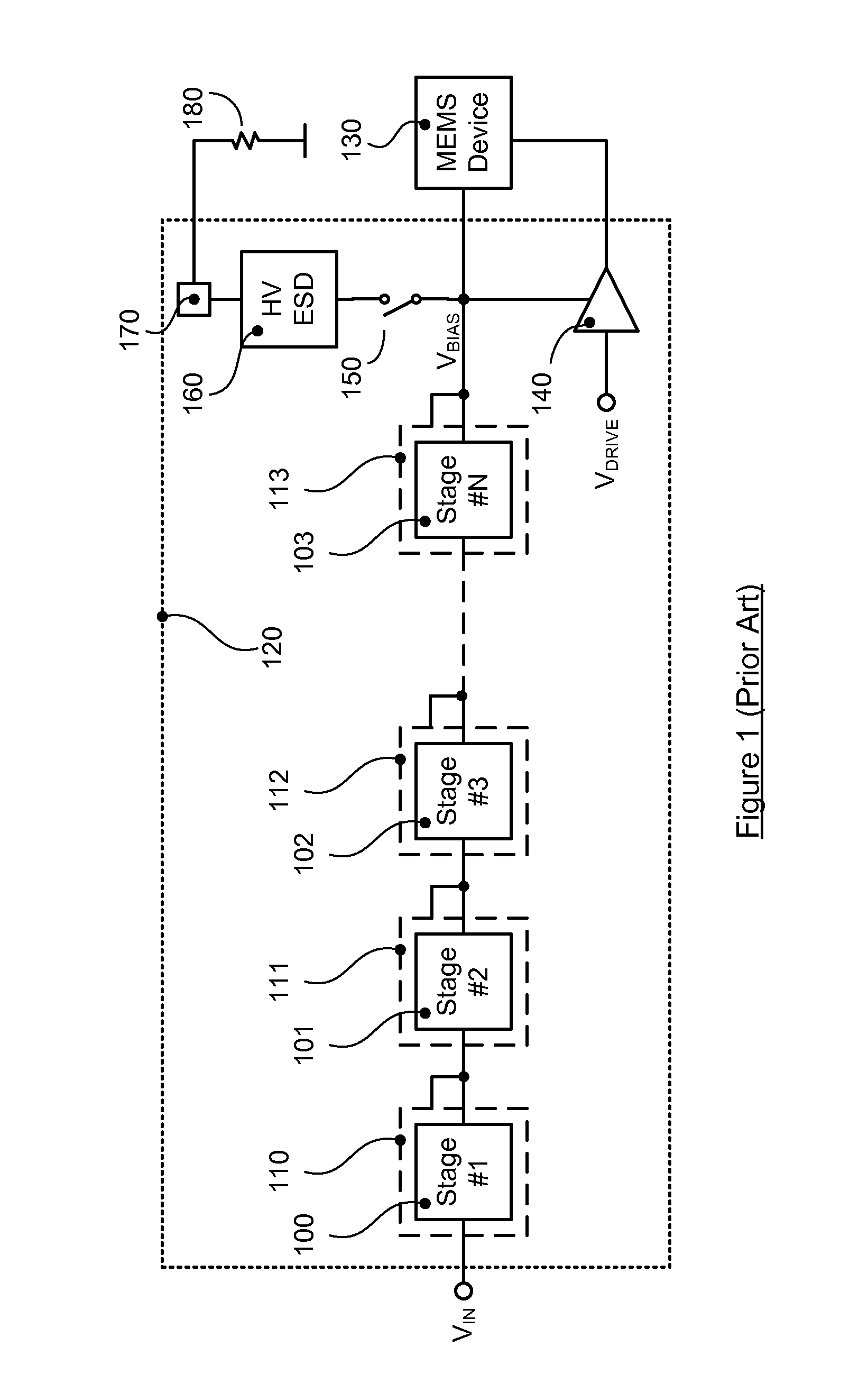
[0018]Some of the complications with using high-voltage biasing can be summarized with reference to FIG. 1, which shows a conventional embodiment of a MEMS system with high-voltage biasing. In this embodiment, a MEMS device 130 connects to a high-voltage bias generator comprising voltage boosting sta...


PUM


Abstract

A high-voltage MEMS system compatible with low-voltage semiconductor process technology is disclosed. The system comprises a MEMS device coupled to a high-voltage bias generator employing an extended-voltage isolation residing in a semiconductor technology substrate. The system avoids the use of high-voltage transistors so that special high-voltage processing steps are not required of the semiconductor technology, thereby reducing process cost and complexity. MEMS testing capability is addressed with a self-test circuit allowing modulation of the bias voltage and current so that a need for external high-voltage connections and associated electro-static discharge protection circuitry are also avoided.

Description

FIELD OF THE INVENTION[0001]The present invention relates generally to MEMS devices and specifically to a method and system for utilizing a MEMS device in a high voltage environment.BACKGROUND OF THE INVENTION[0002]Microelectromechanical (MEMS) devices are used in a variety of applications including solid-state accelerometers, gyroscopes and pressure sensors. MEMS devices used in these applications often make use of capacitive sensing to determine the displacement of the MEMS structure when it is acted on by various forces. For example, an accelerometer senses the acceleration of the MEMS device along a certain axis of motion. Acceleration causes a displacement of a MEMS proof mass which might be sensed by detecting a change in the capacitance between that proof mass and a fixed electrode. In a pressure sensor, a displacement might be caused by a change in pressure and this change can also be sensed capacitively in some implementations. Gyroscopes make similar use of capacitive sens...

Claims


Application Information

Patent Timeline
Patent Type & Authority Applications(United States)
IPC IPC(8): G05F1/10H01L29/06
CPCH01L21/823892H01L27/092B81B2207/015B81B7/008
Inventor SHAEFFER, DEREKCAGDASER, BARISSEEGER, JOSEPH
Owner INVENSENSE
Why Eureka
Try Eureka