Embedded EEPROM array techniques for higher density

a technology of eeprom array and eeprom array, which is applied in the field of single-level poly and floating-gate eeprom array structures, can solve the problems of enabling writing to unselected memory cells, and achieve the effect of reducing wafer area and simplifying structur

Active Publication Date: 2008-12-30
TEXAS INSTR INC
View PDF17 Cites 39 Cited by
  • Summary
  • Abstract
  • Description
  • Claims
  • Application Information

AI Technical Summary

Benefits of technology

[0013]The following presents a simplified summary in order to provide a basic understanding of one or more aspects of the invention. This summary is not an extensive overview of the invention, and is neither intended to identify key or critical elements of the invention, nor to delineate the scope thereof. Rather, the primary purpose of the summary is to present some concepts of the invention in a simplified form as a prelude to the more detailed description that is presented later. The invention relates to an array structure of single-level poly EEPROM memory cells (e.g., NMOS memory cells) and method of operating the array. The EEPROM array is implemented in a higher density embedded EEPROM layout that eliminates the use of high voltage transistors from the array core region. If the high voltage transistors are utilized, they are moved to row and column drivers in the periphery region to increase array density in the core region with little or no added process complexity. This arrangement permits economic implementation of larger embedded SLP EEPROM arrays that have minimal process complexity. During program or erase operations of the array, the method provides a programming voltage comprising first and second half-write voltages associated with the row and column driver circuits, respectively, that are applied to the selected memory cells of the array, and one of the first and second half-write (e.g., mid-level, half-programming) voltages or less applied to the remaining unselected memory cells. Beneficially, this half-write method of operation further enables the operation of a lower voltage driver transistor, does not enable writing to the unselected memory cells, and avoids disturbing the unselected memory cells of the array.
[0015]The half-write scheme of the present invention relies on the principle that the magnitude of the F-N tunneling current at the half-write voltage (e.g., about half the programming voltage) is small enough that non-selected bits are not written into or otherwise disturbed. The half-write scheme of the present invention is compatible with most existing SLP EEPROM schematic cell designs. The number of lead wires or interconnections per row and per column will vary depending on the cell design selected. The half-write scheme puts less voltage stress on some circuit nodes and allows the use of new smaller SLP EEPROM bits. The methods and structure described herein are applicable to silicon wafer fabrication and other such fabrication processes in the manufacture of semiconductor memory devices.
[0017]For example, the half-write method of the present invention enables the transistors of the core to be fabricated from low voltage devices (e.g., 3.3 volt transistors) that operate for a short period of time at nearly double that voltage (e.g., about 6 volts, a half-write voltage level). Then, by combining the half-write voltage applied to a row (e.g., about +6 volts), with another (complementary) half-write voltage applied to a column of cells (e.g., about −6 volts), a higher differential voltage (e.g., about 12 volts) is obtained across a selected cell, or group of cells, suitable to program or erase the selected memory cell(s).
[0018]A cell is programmed, for example, by applying one polarity voltage to the cell (e.g., about +12 volts), while the cell is erased by applying the opposite polarity programming voltage to the cell (e.g., about −12 volts). Similarly, the innovative method of the present invention further enables the row and column driver circuits to be fabricated using conventional lower voltage CMOS transistors in the level-shifter circuits, which traditionally use high voltage transistors. This is because these circuits now only need to withstand the half-write voltage levels (e.g., about 6 volts) for then only for a short period of time. Further, any number of cells of the array may be programmed or erased in this manner by selecting and applying programming voltage levels to any number of rows and columns associated with the selected cells, which will apply no more than about the half-write voltage or less (down to and including no voltage) to the unselected cells.
[0030]In still another aspect of the invention, the semiconductor process may use a dielectric isolated technology for SLP EEPROM where no junction in the array sees more than the half-write voltage, to further simplify structures and reduce the wafer area.

Problems solved by technology

Beneficially, this half-write method of operation further enables the operation of a lower voltage driver transistor, does not enable writing to the unselected memory cells, and avoids disturbing the unselected memory cells of the array.
In addition, this is particularly unexpected when implemented in a conventional digital CMOS process with no added wafer processing steps.

Method used


Image

  • Embedded EEPROM array techniques for higher density
  • Embedded EEPROM array techniques for higher density
  • Embedded EEPROM array techniques for higher density

Examples


Embodiment Construction

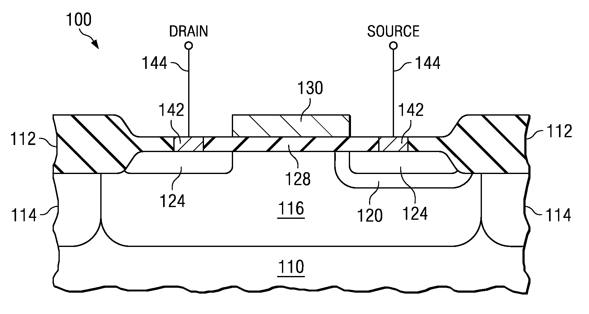
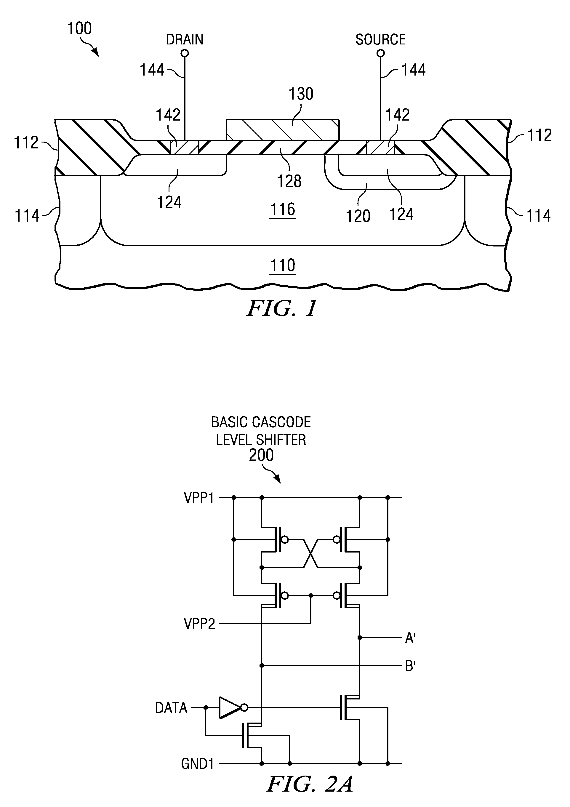
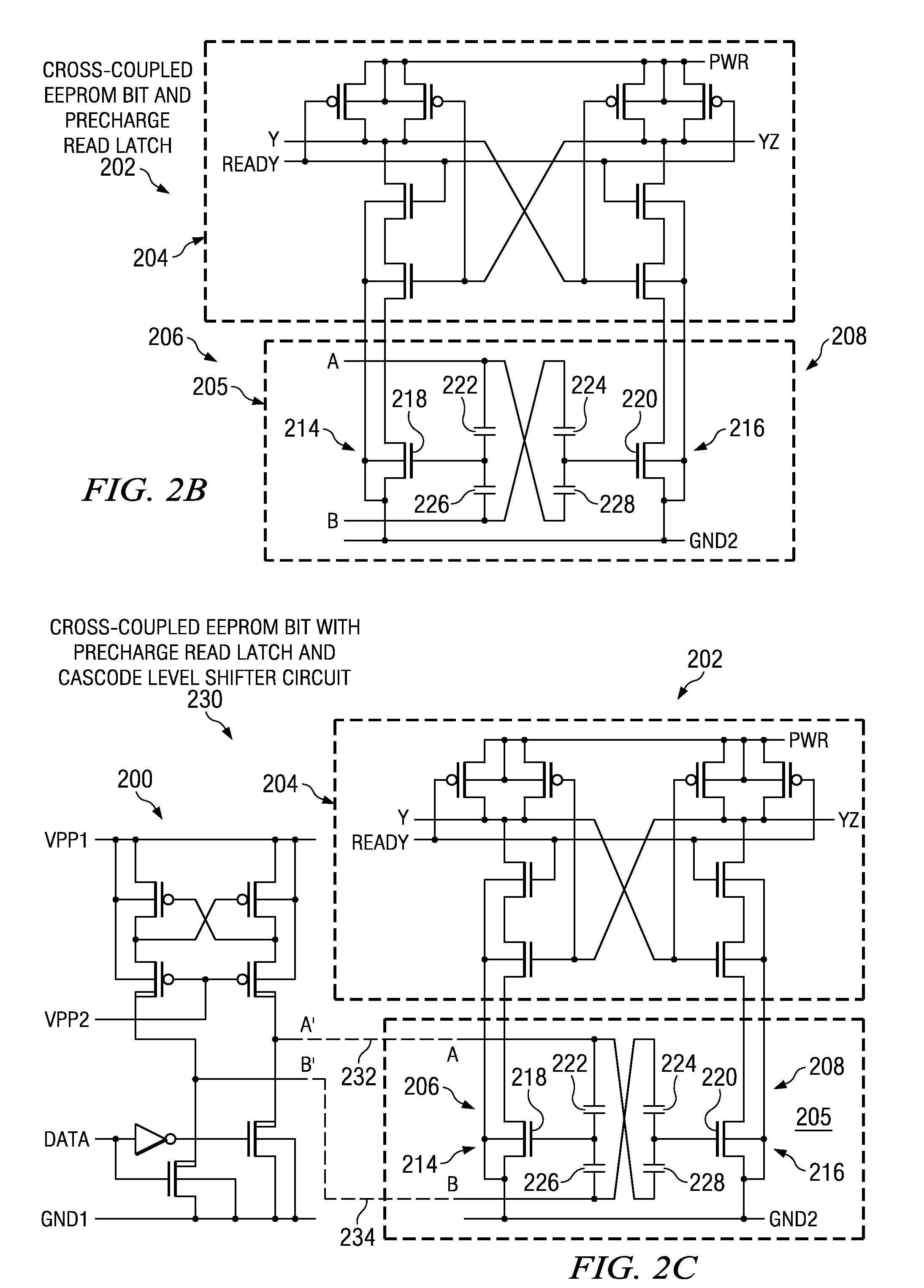
[0050]The present invention will now be described with reference to the attached drawings, wherein like reference numerals are used to refer to like elements throughout. The invention provides an improved embedded EEPROM array structure comprising single-level polysilicon (SLP) EEPROM memory cells (e.g., nMOS and pMOS cells) utilizing floating-gate storage technology. The array of EEPROM memory cells are programmed and erased using a novel half-write programming method. In the half-write programming scheme, row and column drivers of the array apply a full recommended programming voltage (VPP) across selected cells to be programmed or erased and also apply a half-write or mid-level voltage (e.g., half the programming voltage, VPP / 2) or zero voltage to the remaining unselected cells of the array. The half-write voltage VPP / 2 avoids disturbing the unselected cells and limits the voltage between any two rows or columns (or nodes) to the half-write voltage level. An unexpected result of ...


PUM


Abstract

An array structure of single-level poly NMOS EEPROM memory cells and method of operating the array is discussed implemented in a higher density embedded EEPROM layout that eliminates the use of high voltage transistors from the array core region. If they are utilized, the high voltage transistors are moved to row and column drivers in the periphery region to increase array density with little or no added process complexity to allow economic implementation of larger embedded SLP EEPROM arrays. During program or erase operations of the array, the method provides a programming voltage for the selected memory cells of the array, and a half-write (e.g., mid-level) voltage to the remaining unselected memory cells to avoid disturbing the unselected memory cells of the array.

Description

FIELD OF INVENTION[0001]The present invention relates generally to nonvolatile memory (NVM) semiconductor devices and more particularly to single-level poly, floating-gate EEPROM array structures and a method of operating the EEPROM array, implemented in an array layout that eliminates the high voltage transistors from the core area to increase array density with little or no added process complexity, and drives the unselected memory cells of the array to a half-write voltage or less during program and erase operations to avoid disturbing the unselected memory cells of semiconductor devices.BACKGROUND OF THE INVENTION[0002]Current trends in the semiconductor and electronics industry require memory devices to be made smaller, faster and require less power consumption. One reason for these trends is that more personal devices are being manufactured that are relatively small and portable, thereby relying on battery power. In addition to being smaller and more portable, personal devices...

Claims


Application Information

Patent Timeline
Patent Type & Authority Patents(United States)
IPC IPC(8): G11C11/34
CPCG11C16/0416G11C16/0433G11C16/0441G11C16/3418G11C16/3427G11C2216/10H01L29/7881H10B41/10H10B41/60H10B69/00
Inventor MORTON, ALEC JAMESMITROS, JOZEF CZESLAW
Owner TEXAS INSTR INC
Why Eureka
Try Eureka