Heat radiation device for memory module

a memory module and radiation device technology, applied in semiconductor devices, semiconductor/solid-state device details, cooling/ventilation/heating modifications, etc., can solve problems such as thermal breakage of memory elements, memory elements causing system malfunction, and temperature difference among a plurality of adjacent modules is not uniform, so as to achieve efficient radiation of heat generated

Inactive Publication Date: 2007-08-14
LONGITUDE LICENSING LTD
View PDF15 Cites 24 Cited by
  • Summary
  • Abstract
  • Description
  • Claims
  • Application Information

AI Technical Summary

Benefits of technology

[0010]An object of the present invention is to provide a heat radiation device for memory modules which is capable of efficiently radiating heat generated from a plurality of memory modules that are adjacently placed in parallel and at the same time, of unionizing the temperature of each of the memory modules.

Problems solved by technology

In addition, the structure as shown in FIG. 2 may or may not uniformity the temperature difference among modules 2a to 2c, but the temperature difference among a plurality of adjacent modules is not uniformed.
The scattering of characteristic parameters of the memory elements induces system malfunction.
Further, if working frequency of memory elements further increases hereafter, there is also a danger of thermal breakage of memory elements.

Method used


Image

  • Heat radiation device for memory module
  • Heat radiation device for memory module
  • Heat radiation device for memory module

Examples


first embodiment

of the Present Invention

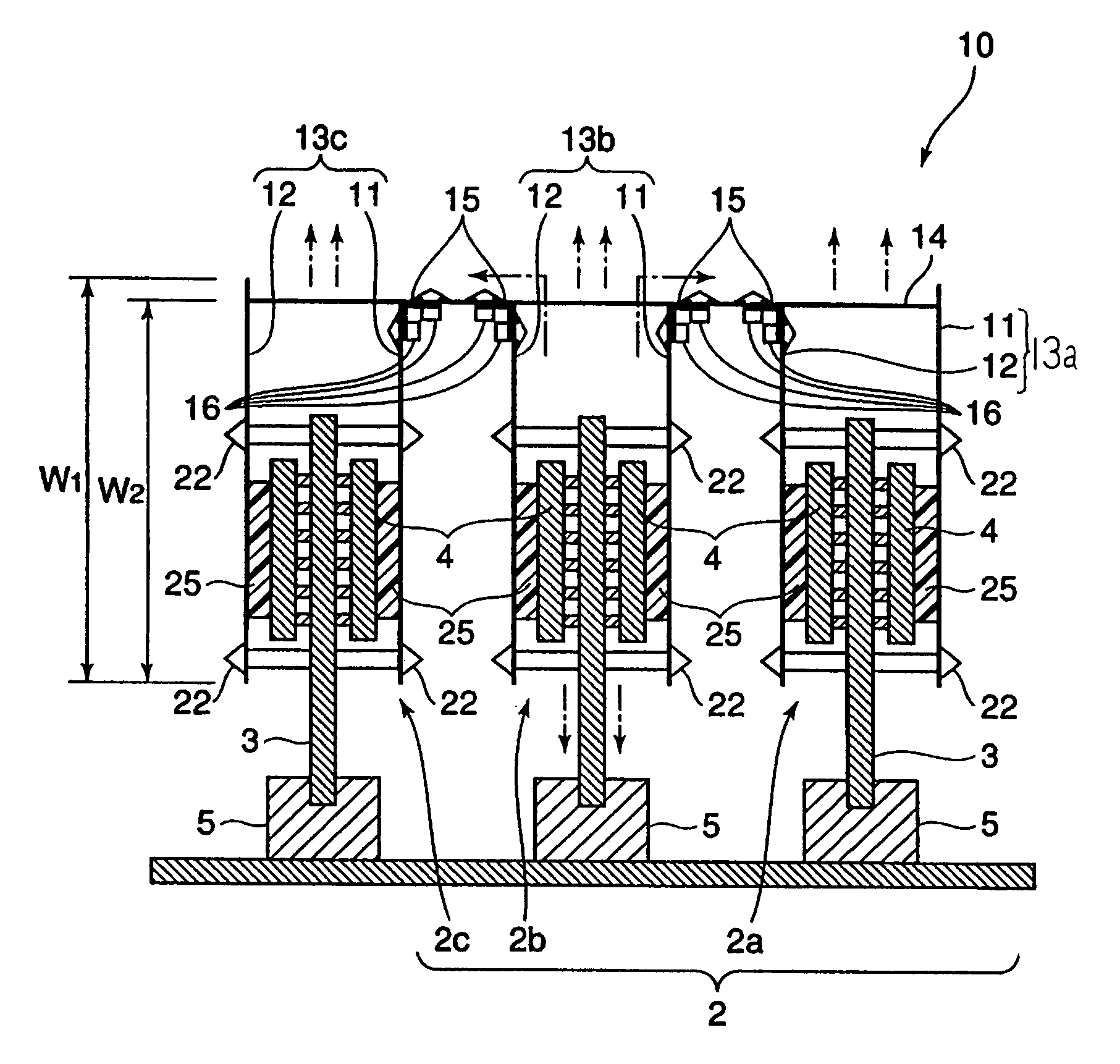
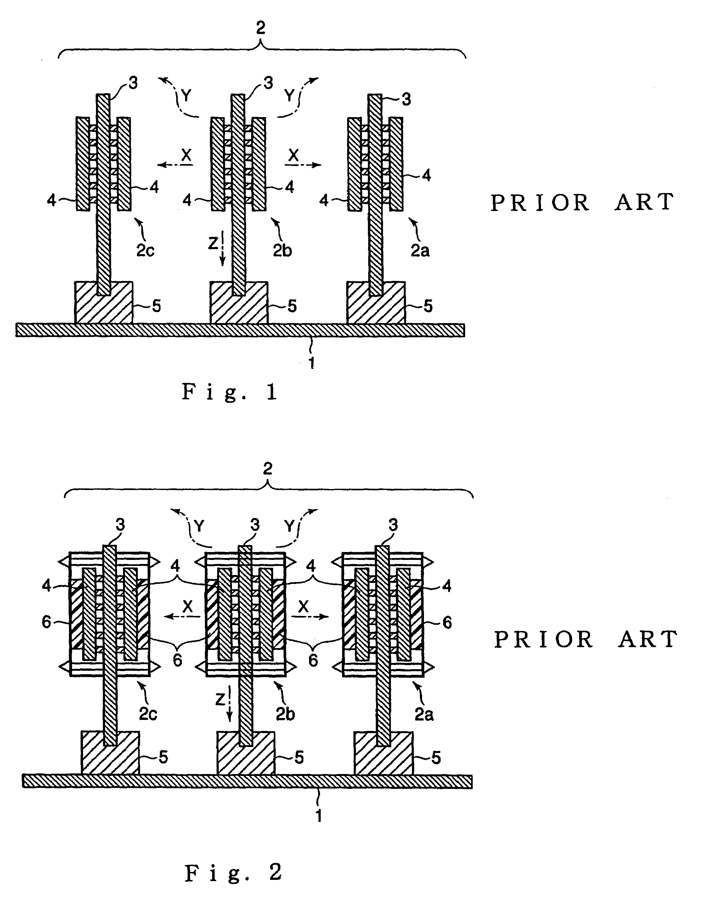
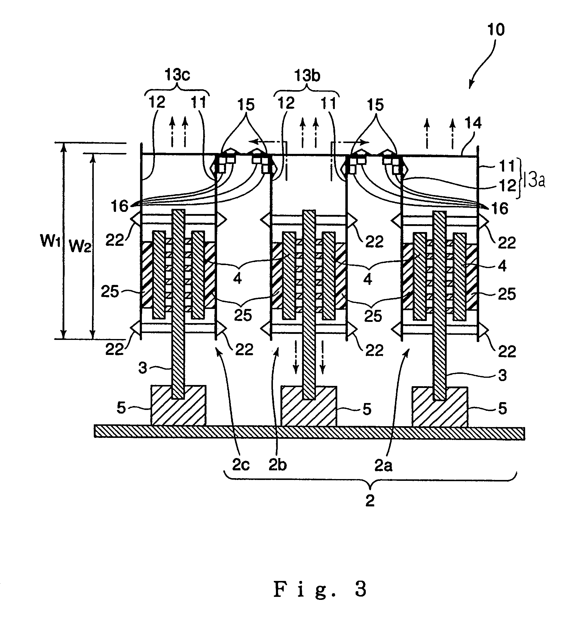
[0025]FIG. 3 is an enlarged cross-sectional view illustrating heat radiation device 10 for memory modules installed on memory module group 2 having three memory modules 2a to 2c according to the present invention. FIG. 4A is a plan view illustrating heat radiation device 10 for memory modules installed on memory module group 2 according to the present invention. FIG. 4B is a partially cutaway side view illustrating heat radiation device 10 for memory modules installed on memory module group 2 according to the present invention, wherein mother board 1 and connector 5 as illustrated in FIG. 3 are not shown in this drawing for the sake of convenience. Memory module group 2 and each of memory modules 2a to 2c which constitute memory module group 2, each shown in FIG. 3, have structures that are the same as those of the memory module group and the memory modules that are shown in FIG. 1. As such, the same structure is marked with the same symbol without repeating ...

second embodiment

of the Present Invention

[0036]Another embodiment of a heat radiation device for memory modules according to the present invention is illustrated in FIG. 6. The fundamental structure of heat radiation device 10 for memory modules shown in FIG. 6 is the same as that of heat radiation device 10 for memory modules shown in FIG. 3. The same structure is marked with the same symbols without repeating the same description, but a description is made only for different structures.

[0037]In regard to heat radiation device 10 for memory modules shown in FIG. 6, front face side heat radiation plates 11 / rear face side heat radiation plates 12, each constituting heat radiation plates in pairs 13a to 13c and memory substrates 3, are connected by an elastic body (spring 40). Thereby front face side heat radiation plates 11 and rear face side heat radiation plates 12 are attracted to the opposite side of memory substrates 3, and closely adhere to the surfaces of memory elements 4 on memory substrates...

third embodiment

of the Present Invention

[0039]Another embodiment of a heat radiation device for memory modules according to the present invention is illustrated in FIG. 7. The fundamental structure of heat radiation device 10 for memory modules shown in FIG. 7 is the same as that of heat radiation device 10 for memory modules shown in FIG. 3. The same structure is marked with the same symbols without repeating the same description, but a description is made only for different structures.

[0040]The memory module shown in FIG. 7 is characterized mainly by an improvement that enables each of memory modules 2a to 2c to be installed on memory module group 2 equipped in advance with heat radiation plate 6. Specifically, the gap between front face side heat radiation plates 11 and rear face side heat radiation plates 12 each constituting radiation plates in pairs 13a to 13c is increased by a necessary and sufficient degree as compared with heat radiation plates in pairs 13a to 13c shown in FIG. 3.

[0041]The...


PUM


Abstract

There is disclosed a heat radiation device for memory modules intended for radiating heat that is generated from a memory module group wherein a plurality of memory modules equipped with memory elements on both the front and rear face sides of a substrate are placed in parallel. The device comprises heat radiation plates in pairs composed of front face side heat radiation plates in contact with memory elements that are installed on the front face side of the substrate for each of the memory modules, and of rear face side heat radiation plates in contact with memory elements that are installed on the rear face side of the substrate; and connecting members for heat radiation plates in pairs which connect the heat radiation plates in pairs so that heat is conducted among a plurality of the heat radiation plates in pairs.

Description

BACKGROUND OF THE INVENTION[0001]1. Field of the Invention[0002]The present invention relates to a heat radiation device for memory modules which radiates heat that is generated from memory elements of each of the modules to cool the memory elements, in cases where a plurality of semiconductor memory modules, wherein a plurality of memory elements are installed on a memory substrate (hereinafter sometimes abbreviated to “module”), are placed in parallel on a mother board or the like to form a module group. The above-mentioned semiconductor memory modules are shown as an example, by DIM (Dual Incline Memory module) wherein a plurality of SCRAM (Synchronous Dynamic Access Memory) are arranged on a memory substrate.[0003]2. Description of the Related Art[0004]An example of a module group is shown in FIG. 1. Module group 2 shown in FIG. 1 consists of three modules 2a to 2c. Each of modules 2a to 2c has memory substrate 3 and a plurality of (generally 16 numbers) memory elements 4 that a...

Claims


Application Information

Patent Timeline
Patent Type & Authority Patents(United States)
IPC IPC(8): H05K7/20H01L23/367H01L23/40H01L25/00H01L25/065
CPCH01L23/3672H01L23/4006H01L25/0652H01L2023/4056H01L2023/4062H01L2023/4068H01L2023/4081H01L2924/0002H01L2924/00
Inventor NAGAHASHI, HARUKI
Owner LONGITUDE LICENSING LTD
Why Eureka
Try Eureka