Non-volatile memory device, and multi-page program, read and copyback program method thereof

a non-volatile memory and program technology, applied in the direction of static storage, digital storage, instruments, etc., can solve the problem of a lower efficiency of the cache program method

Active Publication Date: 2007-08-14
SK HYNIX INC
View PDF3 Cites 114 Cited by
  • Summary
  • Abstract
  • Description
  • Claims
  • Application Information

AI Technical Summary

Benefits of technology

[0012]An advantage of the present invention is a NAND-type flash memory device having a multi-plane structure, in which cells connected to an even bit line within one page and memory cells connected to an odd bit line can be programmed, read, and copyback programmed at the same time.
[0013]According to one embodiment of the present invention, a non-volatile memory device includes a cell array having memory cells respectively connected to word lines and bit lines, a plurality of even page buffers respectively connected to even bit lines of the bit lines through even sensing lines, and a plurality of odd page buffers respectively connected to odd bit lines of the bit lines through odd sensing lines separated from the even sensing lines. In this case, the plurality of even page buffers and the plurality of odd page buffers sequentially receives data to be programmed and programs the data into even memory cells and odd memory cells connected to one word line of the word lines at the same time.
[0014]According to another embodiment of the present invention, a multi-page program method of a non-volatile memory device having a cell array consisting of memory cells respectively connected to word lines and bit lines includes the steps of sequentially storing data to be programmed in a plurality of even page buffers respectively connected to even bit lines of the bit lines through even sensing lines, respectively, and a plurality of odd page buffers respectively connected to odd bit lines of the bit lines through the odd sensing lines, respectively, which are separated from the even sensing lines, and simultaneously programming the data to be programmed, which are stored in the plurality of even and odd page buffers, respectively, into even memory cells and odd memory cells connected to one word line of the word lines.
[0015]According to still another embodiment of the present invention, a multi-page read method of a non-volatile memory device having a cell array consisting of memory cells respectively connected to word lines and bit lines includes the steps of precharging odd bit lines, thus making the odd bit lines shielding bit lines, reading data programmed into even memory cells connected to one word line and storing the data into each of a plurality of even page buffers, precharging the even bit lines that have been sensed, thus making the even bit lines shielding bit lines, reading data programmed into odd memory cells connected to the one word line and storing the data in each of a plurality of odd page buffers, and sequentially reading the data stored in each of the plurality of even and odd page buffers toward the outside.
[0016]According to still another embodiment of the present invention, a multi-page copyback program method of a non-volatile memory device having a cell array consisting of memory cells respectively connected to word lines and bit lines includes the steps of precharging each of odd bit lines of the bit lines, thus making the odd bit lines shielding bit lines, reading data programmed into even memory cells connected to one word line of the word lines and storing the read data in each of a plurality of even page buffers respectively connected to even bit lines of the bit lines through even sensing lines, precharging each of the even bit lines, thus making the even bit lines shielding bit lines, reading data programmed into odd memory cells connected to the one word line and storing the read data in a plurality of odd page buffers respectively connected to the odd bit line through each of odd sensing lines separated from the even sensing lines, and copyback programming the data stored in each of the plurality of even page buffers and the data stored in each of the plurality of odd page buffers into even memory cells and odd memory cells connected to the other word line of the word lines.

Problems solved by technology

The cache program method has, however, a lower efficiency as the program time of the cell is higher than the data input time.

Method used


Image

  • Non-volatile memory device, and multi-page program, read and copyback program method thereof
  • Non-volatile memory device, and multi-page program, read and copyback program method thereof
  • Non-volatile memory device, and multi-page program, read and copyback program method thereof

Examples


Embodiment Construction

[0024]Embodiments according to the present invention will be described with reference to the accompanying drawings. Since these embodiments are provided for the purpose that those ordinary skilled in the art are able to understand the present invention, the embodiments may be modified in various manners so that the scope of the present invention is not limited by the embodiments described later.

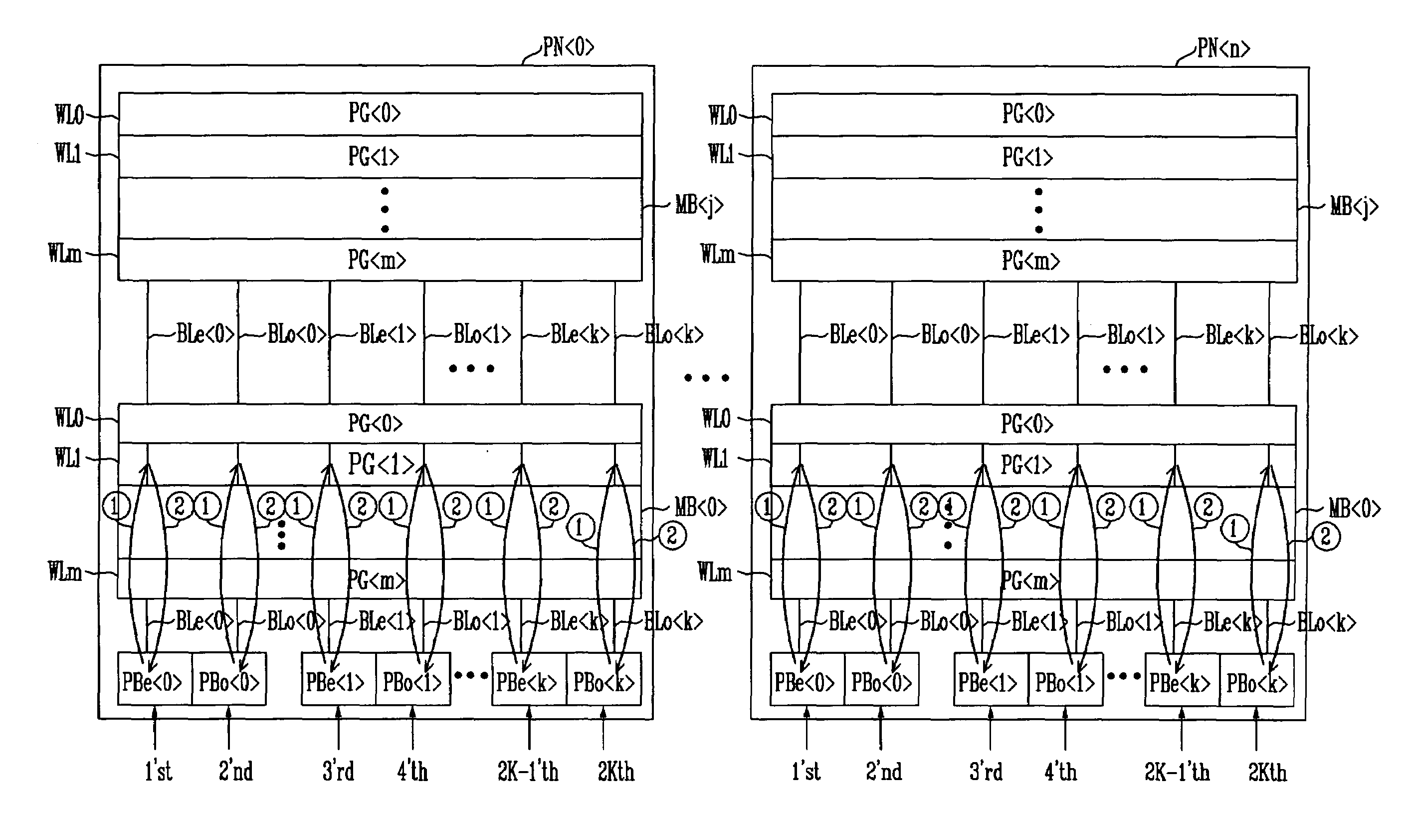
[0025]FIG. 3 is a block diagram of a NAND-type flash memory device having a multi-plane structure according to an embodiment of the present invention.

[0026]Referring to FIG. 3, the NAND-type flash memory device includes N number of planes PN0> to PN. Each of the planes PN0> to PN has J number of memory cell blocks MB0> to MB. Each of the memory cell blocks MB0> to MB includes M number of pagers PG0> to PG, which are controlled by M number of word lines WL0 to WLm, respectively.

[0027]As shown in FIG. 3, 2K number of page buffers PBe0> to PBe and PBo0> to PBo exist in each of the planes PN0> to...


PUM


Abstract

A NAND-type flash memory device has a multi-plane structure. Page buffers are divided into even page buffers and odd page buffers and are driven at the same time. Cells connected to even bit lines within one page and cell connected to odd bit lines within one page are programmed, read and copyback programmed at the same time.

Description

BACKGROUND[0001]1. Field of the Invention[0002]The present invention relates to non-volatile memory devices, and multi-page program, read and copyback program method thereof. More specifically, the present invention relates to non-volatile memory devices having a multi-plane structure, and multi-page program, read and copyback program method thereof.[0003]2. Discussion of Related Art[0004]In the case of NAND-type flash memory devices, the program speed is very slow, i.e., about several hundreds of μs. To improve the program throughput becomes an important parameter representing the performance of chips. In order to enhance the program throughput, various program operation methods such as a cache program and a multi-page program have been proposed. In the case of the cache program, while data are programmed into a cell, next data are previously stored in a page buffer. The cache program method has, however, a lower efficiency as the program time of the cell is higher than the data in...

Claims


Application Information

Patent Timeline
Patent Type & Authority Patents(United States)
IPC IPC(8): G11C11/34G11C16/04
CPCG11C16/0483G11C16/12G11C16/24G11C16/32G11C16/3454G11C2216/14G11C16/06G11C16/10
Inventor PARK, JIN SU
Owner SK HYNIX INC
Why Eureka
Try Eureka