Semiconductor integrated circuit device

a technology of integrated circuit device and semiconductor, which is applied in the direction of solid-state devices, basic electric elements, electrical apparatus construction details, etc., can solve the problems of large radiation noise and ground bounce noise generated by the semiconductor integrated circuit device (ic) on other electronic devices, and the malfunction of the circuit itself has become a large problem, so as to reduce the size of the package and reduce the impedance

Inactive Publication Date: 2007-08-21
CANON KK
View PDF14 Cites 19 Cited by
  • Summary
  • Abstract
  • Description
  • Claims
  • Application Information

AI Technical Summary

Benefits of technology

[0011]It is, therefore, an object of the present invention to provide a semiconductor integrated circuit device comprising therein a highly integrated semiconductor chip and having wire bonding pads arranged in at least two rows in a staggered manner, which semiconductor integrated circuit device can significantly contribute to reduction of impedance for an entire power supply path, and to reduction in size of a package.

Problems solved by technology

In recent years, with the progress of semiconductor fine processing technology involving further enlargement of circuit scale, the adverse affect of radiation noise or ground bounce noise generated from a semiconductor integrated circuit device (IC) on other electronic devices and malfunction of a circuit itself has become a large problem.
Consequently, there has been posed a problem that much radiation noise and ground bounce noise will be generated.

Method used


Image

  • Semiconductor integrated circuit device
  • Semiconductor integrated circuit device
  • Semiconductor integrated circuit device

Examples


example 1

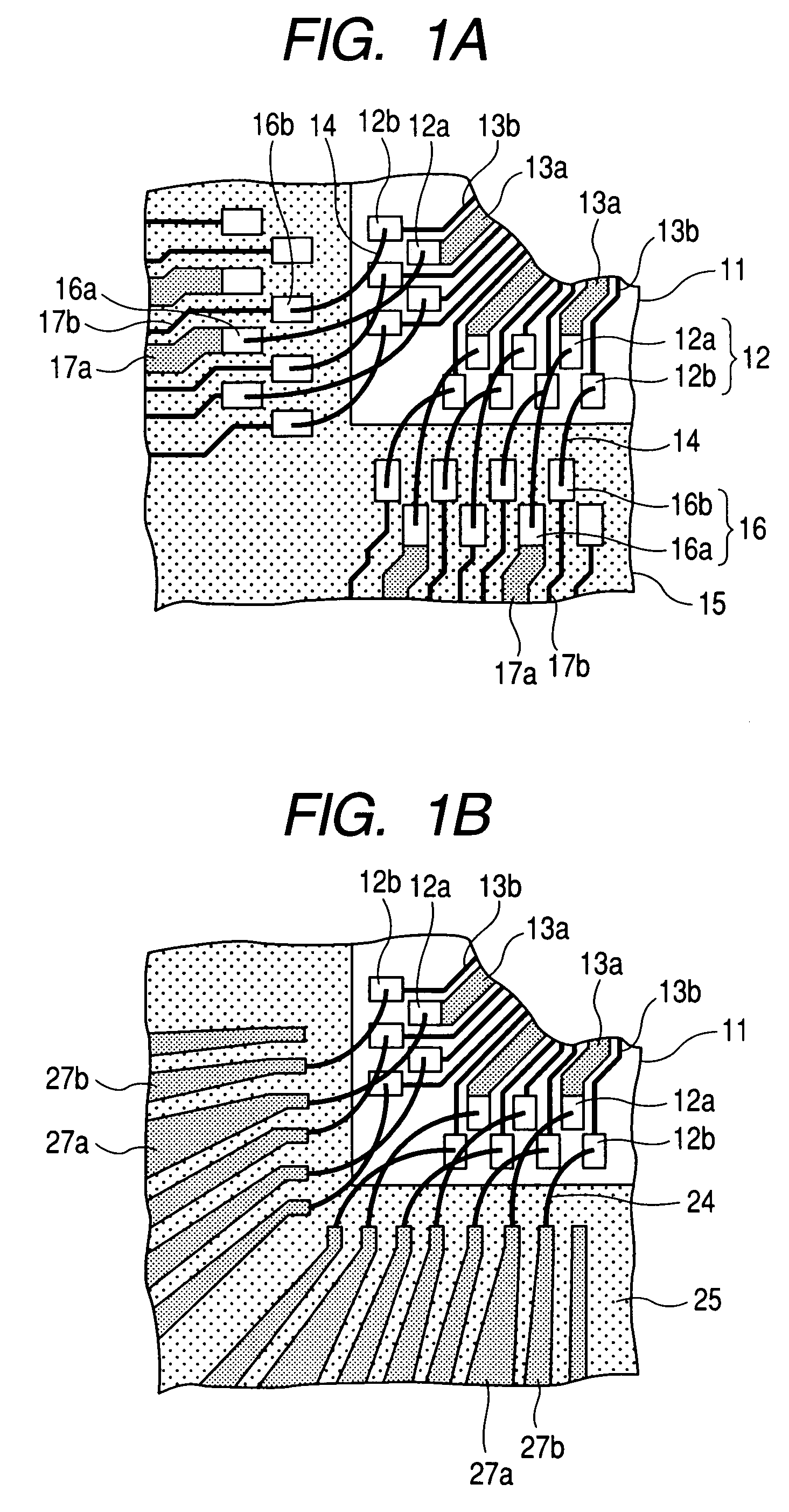
[0028]FIG. 1A is a plan view showing the inside of an IC according to Example 1 of the invention. Wire bonding pads 12 on a semiconductor chip 11 are disposed in two rows in a staggered manner. Of the wire bonding pads 12, power supply pads 12a (power pad and ground pad) are all assigned to the wire bonding pads in a rear row that is located more inside of the semiconductor chip 11. On the other hand, of the wire bonding pads 12, signal pads 12b may be assigned to any of the wire bonding pads. Power supply lines 13a from the power supply pads 12a, and signal lines 13b from the signal pads 12b are connected to a semiconductor integrated circuit unit (not shown) disposed inside the semiconductor chip 11. In this case, the line width of the power supply lines 13a thus disposed is equal to or larger than the width of the power supply pads 12a. The power supply lines 13a from the power supply pads 12a disposed at the rear row that is located more inside of the semiconductor chip 11 are n...

example 2

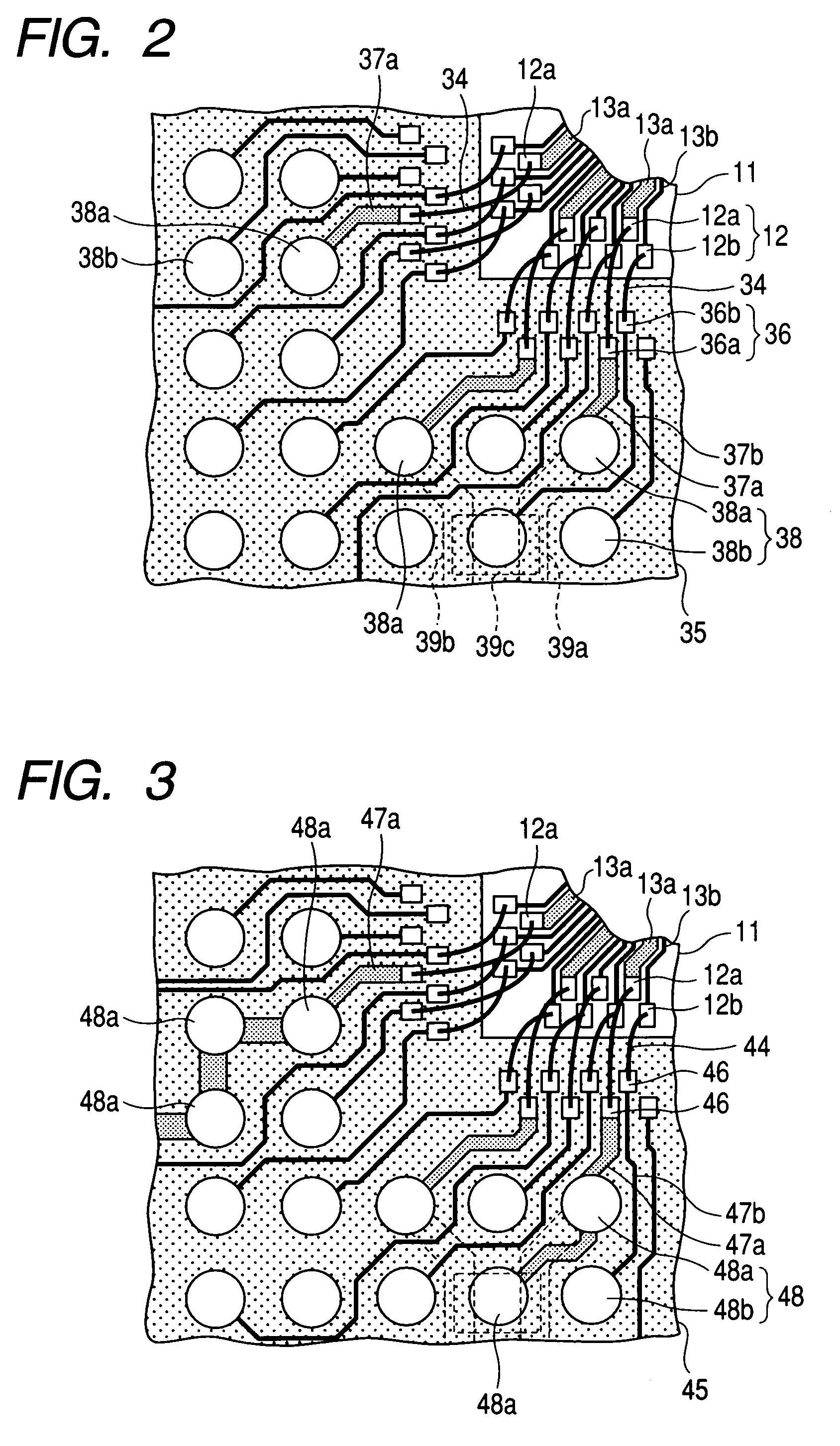
[0033]FIG. 2 is a plan view showing the inside of an IC according to Example 2 of the invention. FIG. 2 shows a case where the package is a BGA (Ball Grid Array). Referring to FIG. 2, the semiconductor chip 11 has a structure similar to the one shown in FIG. 1A. Thus, the same reference numerals are applied to parts corresponding to those in FIG. 1A, and an explanation thereof is omitted.

[0034]In FIG. 2, similarly to Example 1 shown in FIG. 1A, wire bonding pads 36 on package 35 are disposed in two rows in a staggered manner. Of the wire bonding pads 36, power supply pads 36a are all disposed in a rear row that is located more inside of the package 35, and in a front row that is located less inside of the package 35, there are deposed only signal pads 36b. Wire bonding pads 12 on the semiconductor chip 11 are connected via bonding wires 34 to the wire bonding pads 36 on the package 35. With this arrangement, power supply lines 37a each have a large line width led out from the wire b...

example 3

[0038]FIG. 3 is a plan view showing the inside of an IC according to Example 3 of the invention, in which the package is a BGA. Referring to FIG. 3, the semiconductor chip 11 has a structure similar to the one shown in FIG. 1A. Thus, the same reference numerals are applied to parts corresponding to those in FIG. 1A, and an explanation thereof is omitted.

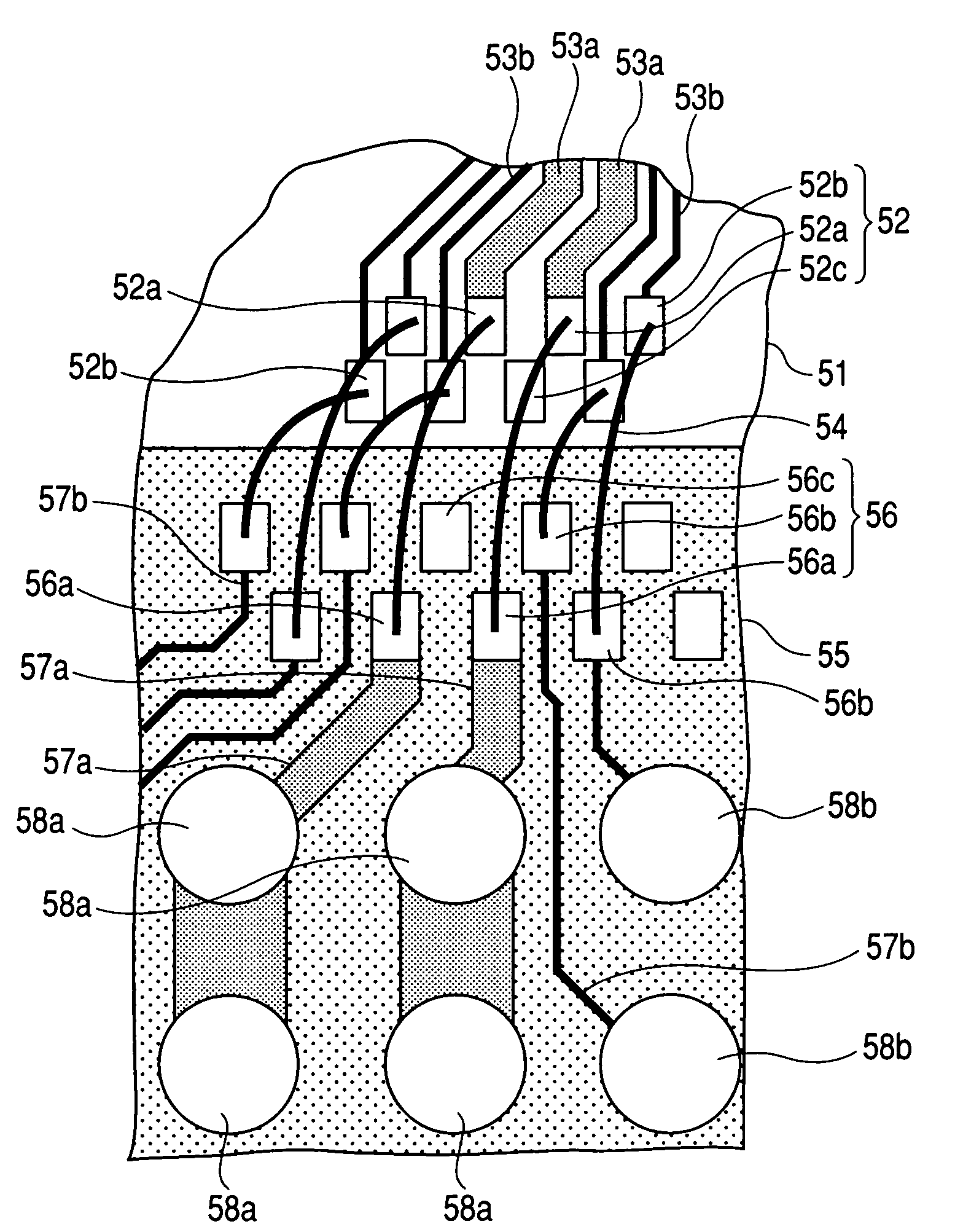
[0039]As shown in FIG. 3, the total number of BGA ball lands 48 provided in a package 45, including power supply lands 48a and signal lands 48b used to connect to the printed wiring board, is larger than the total number of wire bonding pads 46 used as power supply pad or signal pad. Wire bonding pads 12 on the semiconductor chip 11 are connected via bonding lines 44 to the wire bonding pads 46 on the package 45. A plurality of power supply lands 48a are connected in series to a single power supply line 47a having a large line width led out from the wire bonding pad 46. Accordingly, the impedance of the electrical connection between ...


PUM


Abstract

A semiconductor integrated circuit device is provided which comprises a semiconductor chip having wire bonding pads and a package encapsulating the semiconductor chip and connected via bonding wires to the wire bonding pads, wherein wire bonding pads on the semiconductor chip are arranged in two rows in a staggered manner along a periphery of the semiconductor chip, and of the wire bonding pads, power supply pads are arranged in a rear row located close to a semiconductor integrated circuit unit as an active area on the semiconductor chip and in a front row, only signal pads are arranged. Because the power supply pads are provided in the rear row, the line width of a power supply line led out from each power supply pad can be made equal to the width of the pad, thus reducing the impedance of the connection circuit between the semiconductor chip and the package, and suppressing generation of radiation noise, ground bounce and so on.

Description

BACKGROUND OF THE INVENTION[0001]1. Field of the Invention[0002]The present invention relates to a semiconductor integrated circuit device (IC package) having a semiconductor chip encapsulated with a package comprised of a resin and being capable of suppressing radiation noise or ground bounce noise caused by a connection wiring structure between the semiconductor chip and the package.[0003]2. Related Background Art[0004]In recent years, with the progress of semiconductor fine processing technology involving further enlargement of circuit scale, the adverse affect of radiation noise or ground bounce noise generated from a semiconductor integrated circuit device (IC) on other electronic devices and malfunction of a circuit itself has become a large problem.[0005]The radiation noise or ground bounce noise is caused by the fact that when an internal circuit of an IC operates, a large current flows through a path of a power terminal of a bypass capacitor→a power line of a printed wiring...

Claims


Application Information

Patent Timeline
Patent Type & Authority Patents(United States)
IPC IPC(8): H01L23/52H05K7/10H01L27/04H01L21/60H01L21/822H01L23/48H01L23/498H01L23/50
CPCH01L23/49838H01L24/06H01L24/49H01L23/50H01L2224/05553H01L2224/04042H01L2224/05599H01L2224/06153H01L2224/48091H01L2224/48225H01L2224/4917H01L2224/49171H01L2224/49431H01L2224/49433H01L2224/85399H01L2924/01004H01L2924/01005H01L2924/01006H01L2924/01082H01L2924/14H01L2924/15173H01L2924/19041H01L2924/30107H01L2924/3011H01L2924/01033H01L2924/01023H01L2924/00014H01L24/48H01L2224/45099H01L2924/00H01L2224/023H01L2224/48227H01L2924/12042H01L2924/0001
Inventor INAGAWA, HIDEHO
Owner CANON KK
Why Eureka
Try Eureka