Method and apparatus for built-in self-test (BIST) of integrated circuit device

a self-testing and integrated circuit technology, applied in the direction of electronic circuit testing, measurement devices, instruments, etc., can solve the problems of high cost, conventional bist configurations are not well suited for characterizing timing parameters, and conventional bist configurations provide no emulation of the actual path of signals propagating,

Inactive Publication Date: 2007-09-11
RAMBUS INC
View PDF7 Cites 19 Cited by
  • Summary
  • Abstract
  • Description
  • Claims
  • Application Information

AI Technical Summary

Benefits of technology

[0019]Such an arrangement can result in dual roles for BIST structures; driving BIST data and providing ESD protection. This may provide better BIST capabilities in an advantageously small overall area.
[0025]Such an arrangement can allow for a phase relationship between pipeline controlling signals to be established with a reasonable degree of precision.
[0027]Such an arrangement can generate pass / fail indications that take into account physical input structures effects, as well as emulated timing parameters without necessarily requiring an expensive class type tester.
[0035]Such an arrangement can allow the testing of timing critical parameters with a BIST circuit as opposed to a high cost class tester, or the like.
[0037]Such an arrangement can enable timing parameters for a memory device to be self-tested that take into account the effect of the structure of physical signal inputs. Thus, timing parameters can be checked without having to employ a high cost class tester.

Problems solved by technology

Such an approach can be time consuming as a tester must apply various input signals and wait for the resulting test result signals.
Further, instead of having a tester sequence through various functions and accumulate results, a tester may only have to read a pass or fail indication.
However, conventional BIST configurations are not well suited for characterizing timing parameters.
As a result, conventional BIST configurations provide no emulation of the actual path of signals propagating from the tester through chip bond pads.
Also, many conventional BIST test patterns typically only work for certain critical paths and the overall test coverage relative to a full set of main chip functions and / or states can be low.
As noted above, this can be time consuming, complex, and expensive.
Such testing of timing critical parameters is typically accomplished by a high speed “class” tester that can be very costly to purchase and or operate.

Method used


Image

  • Method and apparatus for built-in self-test (BIST) of integrated circuit device
  • Method and apparatus for built-in self-test (BIST) of integrated circuit device
  • Method and apparatus for built-in self-test (BIST) of integrated circuit device

Examples


first embodiment

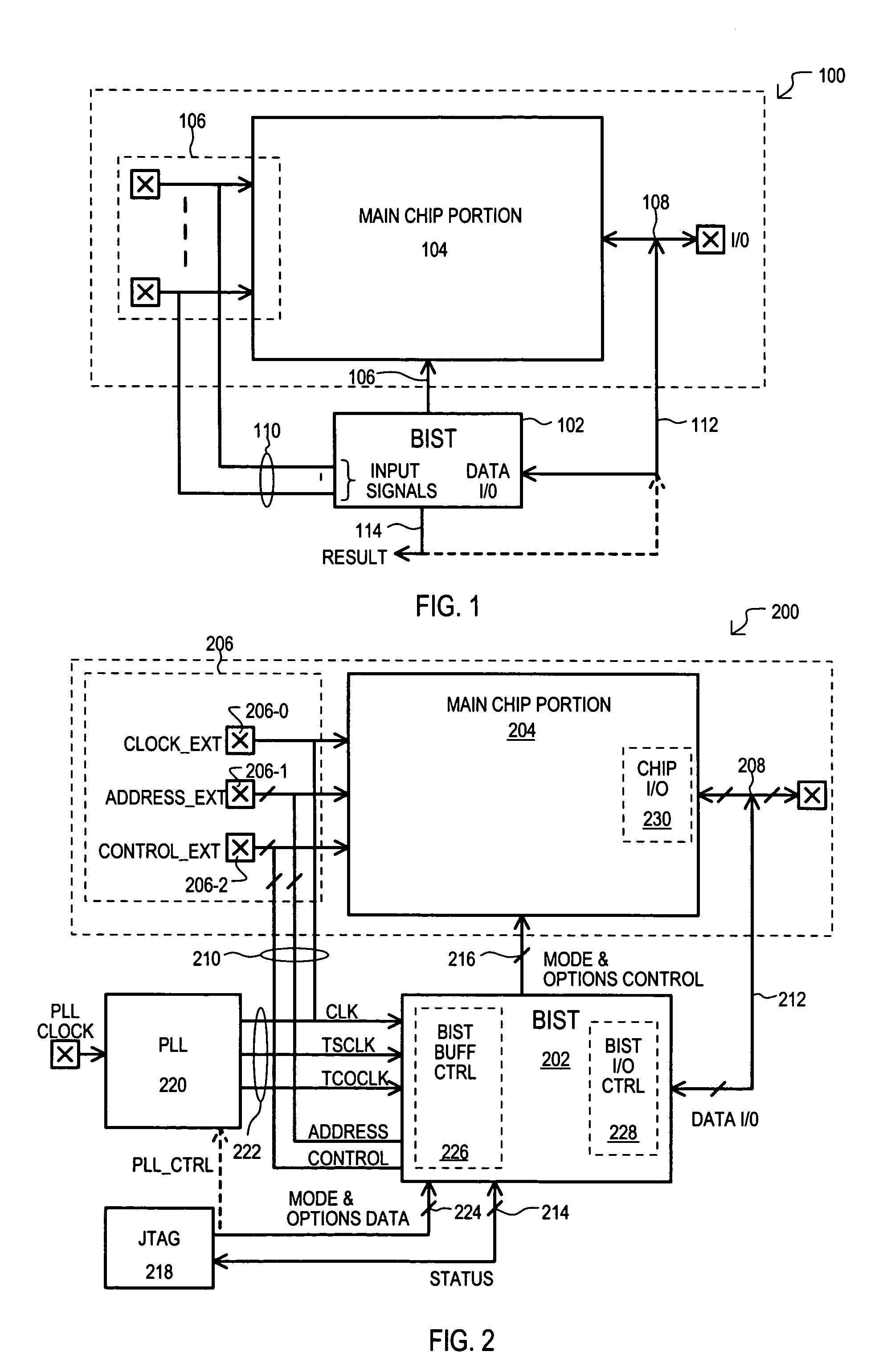
[0049]the present invention is an integrated circuit device (i.e., chip) having a BIST capability. The first embodiment is shown in FIG. 1 in a block schematic diagram and designated by the general reference character 100. A chip 100 can include a BIST block 102, a main chip portion 104, one or more physical input structures 106, and one or more physical input and / or output (I / O) structures 108.

[0050]Unlike a conventional BIST arrangement, like that of FIG. 5, a chip 100 may also include BIST input paths 110 and BIST I / O paths 112. BIST input paths 110 can be connected between physical input structures 106 and BIST block 102. BIST I / O paths 112 can be connected between physical I / O structures 108 and BIST block 102.

[0051]A main chip portion 104 can provide a main chip function according to applied inputs. For example, in response to signals applied at physical input structures 106, a main chip portion can generate / receive signals at physical I / O structures 108. A main chip portion 1...
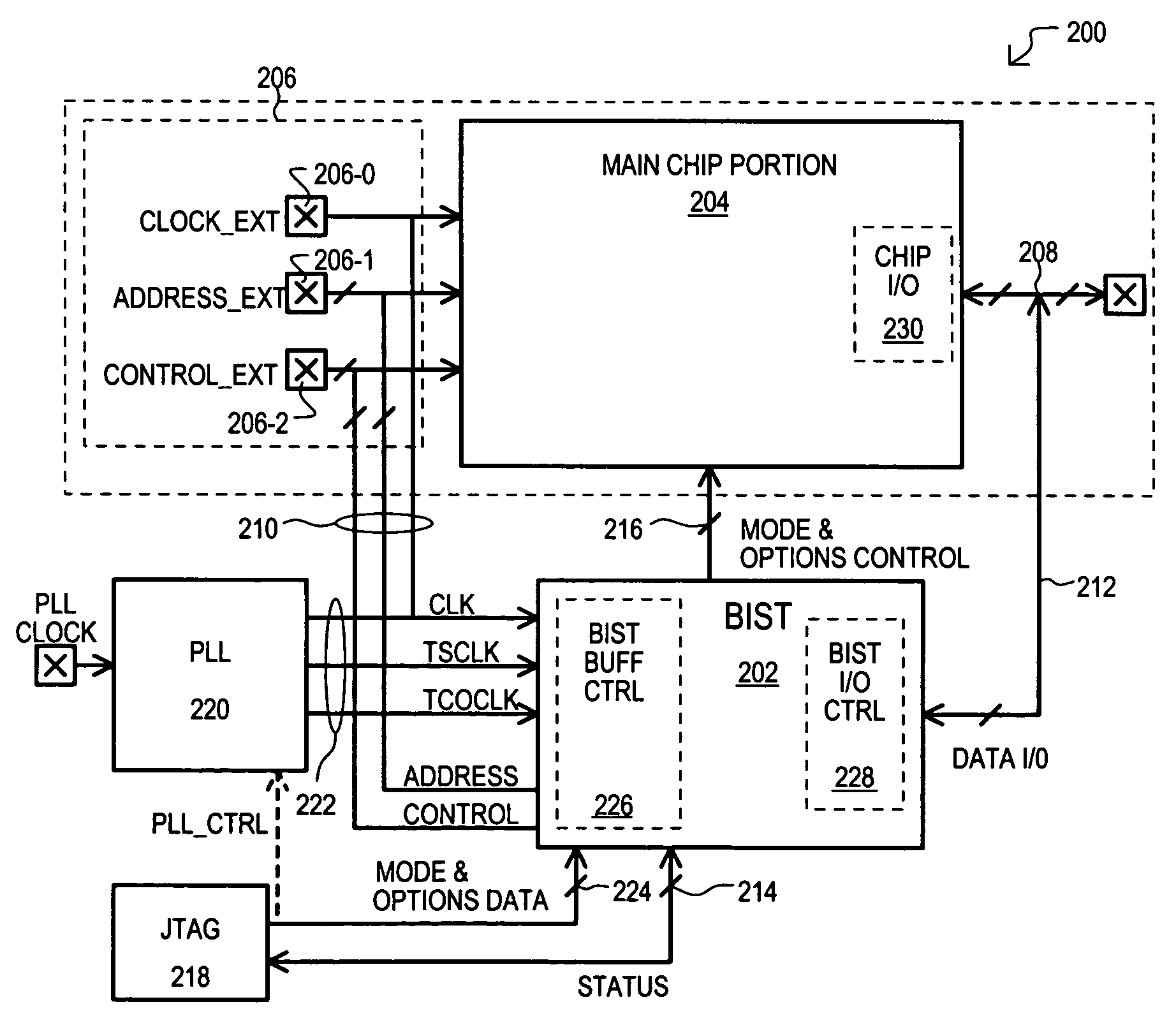
second embodiment

[0073]The general operation of a second embodiment will now be described. A chip may be placed into a test mode by a test set signal being applied via test block and I / F 218. This data state may also be forwarded to BIST block 202 by test I / F path 224. In response BIST block 202 can be activated.

[0074]Test mode signals can be applied to establish a particular test mode state for test block and I / F 218. Again, such data may be utilized to generate MODE & OPTIONS DATA that is forwarded to BIST block 214. In response to such data, BIST block 202 can generate MODE & OPTION CONTROL signals. Such signals can be applied to main chip portion 204 to set a chip 200 into a particular operational mode.

[0075]A PLL clock signal PLL CLOCK can also be applied to PLL type block 220. In response to such a clock, PLL type block 220 can generate clock signals (CLK, TSCLK and TCOCLK) on clock outputs 222. As will be explained at a later point herein, a clock signal CLK, can be an operational clock signa...


PUM


Abstract

An integrated circuit device (200) can include a main portion (204) and a built-in self-test (BIST) portion (204) having outputs coupled to physical input structures (e.g., bond pads) (206) of the integrated circuit device (200). A BIST portion (202) can test timing critical parameters that take into account the effect of input structures (206). A BIST portion (202) can apply BIST test signals with a pipeline structure that can emulate timing parameters, such as a set-up time (Ts) and a clock-to-output time (Tco).

Description

TECHNICAL FIELD[0001]The present invention relates generally to the testing of integrated circuit devices, and more particularly to built-in self-test (BIST) circuitry configured for timing characterization of integrated circuit devices.BACKGROUND OF THE INVENTION[0002]In order to reduce overall integrated circuit (i.e., chip) test costs, many modern chips are fabricated with built-in self-test (BIST) circuitry. Such circuitry is considered “built-in” as it is included on the chip itself. This can allow for internally generated test patterns to be applied to a portion of the chip.[0003]The manufacture of integrated circuit devices can be conceptualized as including a “front-end” and a “back-end.” A manufacturing front end may include the fabrication of devices on a wafer. A back-end may include slicing wafers into dice, packaging the dice, and testing the resulting packages. With the increasing speed and / or complexity of integrated circuit devices, testing can become an important st...

Claims


Application Information

Patent Timeline
Patent Type & Authority Patents(United States)
IPC IPC(8): G01R31/28
CPCG01R31/31725G01R31/3187
Inventor LI, JUNTZOU, JOSEPHTRAN, THINH
Owner RAMBUS INC
Why Eureka
Try Eureka