System, method and program product for well-bias set point adjustment

a well-bias set point and set point adjustment technology, applied in the field of semiconductor devices, can solve the problems of reducing power consumption, and increasing the size of the devices that can be constructed on a semiconductor substra

Active Publication Date: 2007-09-25
NXP USA INC
View PDF10 Cites 28 Cited by
  • Summary
  • Abstract
  • Description
  • Claims
  • Application Information

AI Technical Summary

Problems solved by technology

As semiconductor processes advance, the size of the devices that can be constructed on a semiconductor substrate continues to grow smaller.
In addition, as device sizes shrink, the problem with current leaking between devices, and between various device features, is exacerbated.
Since many handheld products are typically not used for significant periods of time—up to 95% of the time for some products such as cellular phones—controlling the current leakage of semiconductor devices during periods when the product is not in use can result in reduced power consumption.
While providing significant advantages in reducing leakage current, a well-bias circuit applying a negative well-bias can also result in problems during operation.
While the application of a negative well-bias will reduce the transistor leakage currents, its application under certain circumstances can create a reliability issue for the circuits.
When well-bias is applied, the cumulative well-bias and drain-to-source voltages cause various voltage stress effects across the gate-to-body and drain-to-body junctions that reduces component lifetime.
As a result, use of a well-bias circuit may, in some cases, raise reliability concerns with regard to the integrated circuits implementing such systems.

Method used


Image

  • System, method and program product for well-bias set point adjustment
  • System, method and program product for well-bias set point adjustment
  • System, method and program product for well-bias set point adjustment

Examples


Embodiment Construction

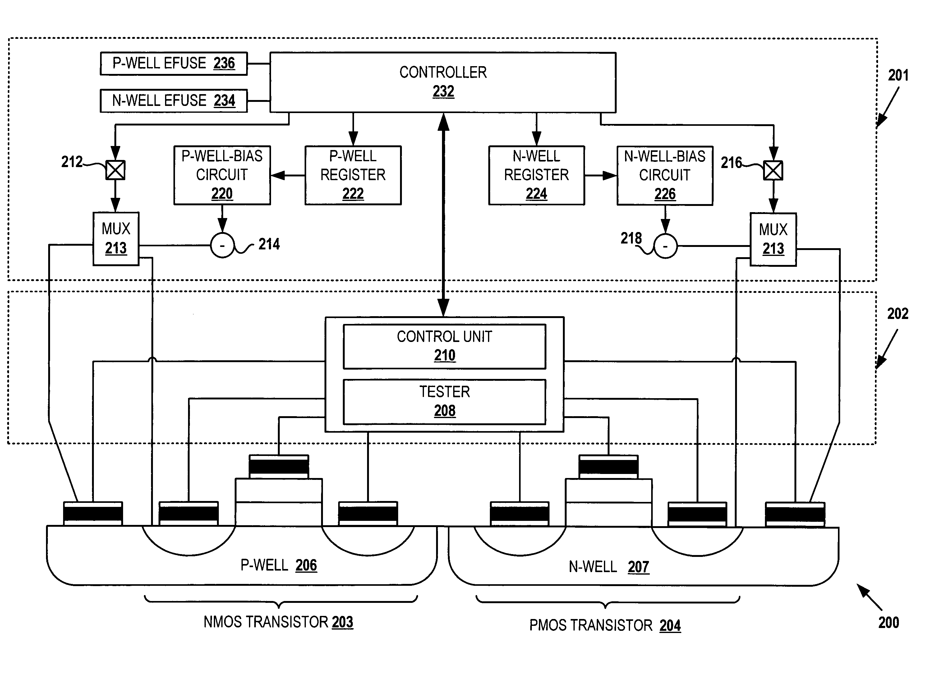
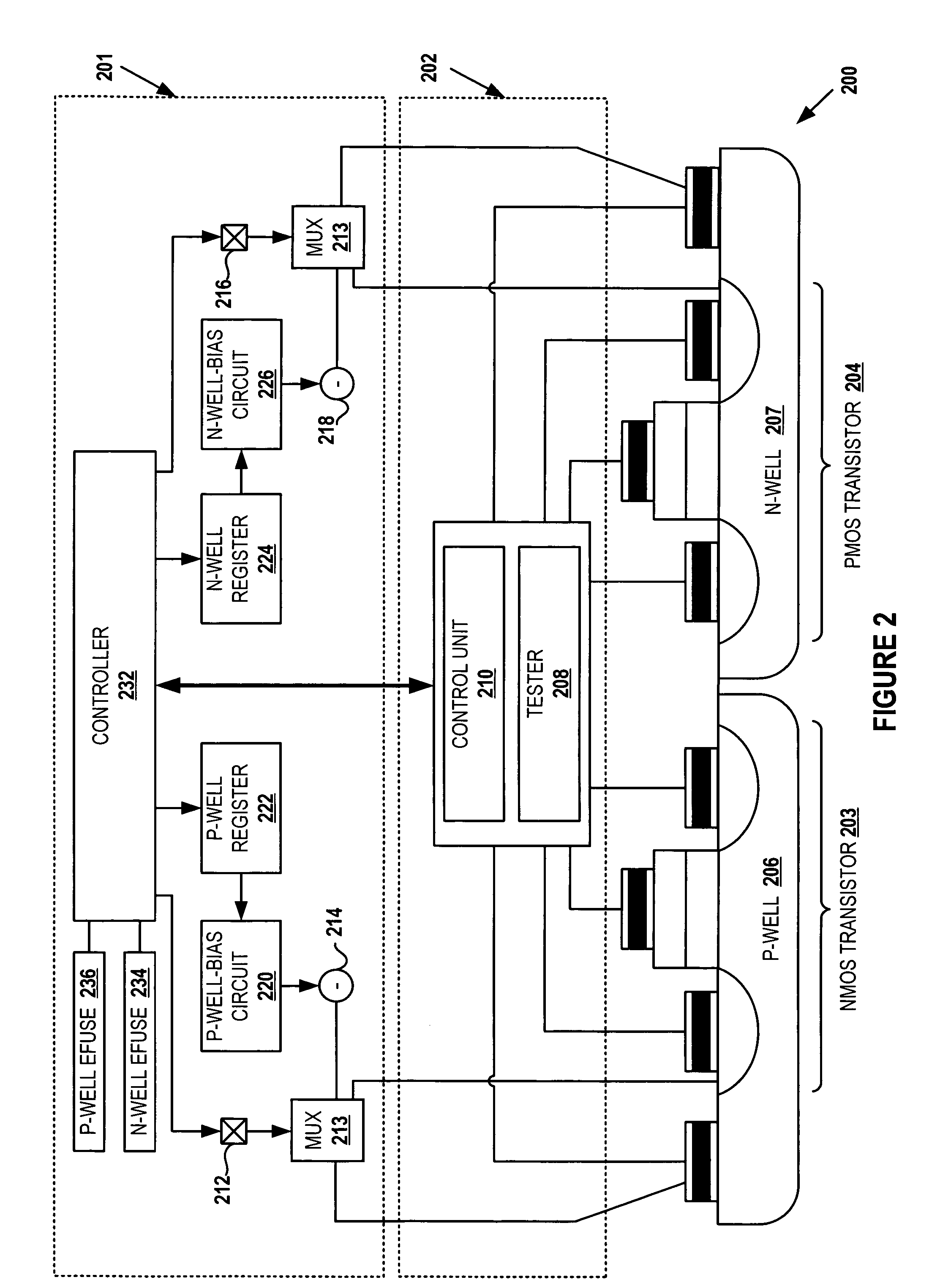
[0016]A preferred embodiment of the present invention provides a mechanism for dynamically adjust the well-bias set points to optimal levels across an integrated circuit (IC) to achieve enhanced power savings and component reliability during a standby or low-power mode of operation. A controller within the IC determines if the chip power supply voltage (e.g., drain / source terminal voltages) will be reduced during an imminent standby or low power mode and sets a register controlling a negative well-bias voltage accordingly. To minimize leakage current without compromising reliability, the well-bias voltage is set to:

[0017](1) optimal well-bias set points if a reduced supply voltage is to be applied to the IC, or

[0018](2) minimum well-bias set points when a nominal or high supply voltage is to be applied to the IC.

[0019]In the following detailed description of exemplary embodiments of the invention, specific exemplary embodiments in which the invention may be practiced are described i...


PUM


Abstract

A well-bias system dynamically adjusts well-bias set points to optimal levels across an integrated circuit (IC) for enhanced power savings and component reliability during a standby or low-power mode of operation. A controller within the IC determines if the chip power supply voltage will be reduced during an imminent standby or low power mode and sets a register controlling a negative well-bias set point for asserting well-bias to charge wells of the IC accordingly. To minimize leakage current without compromising reliability, the well-bias set point is set to (1) an optimal well-bias set point if a reduced supply voltage is to be applied to the IC, or (2) a minimum well-bias set point when a nominal or high supply voltage is to be applied to the IC.

Description

BACKGROUND OF THE INVENTION[0001]1. Field of the Invention[0002]The present invention relates generally to semiconductor devices, and more particularly, to a system and method for dynamically adjusting well-bias of transistors in an integrated circuit.[0003]2. Description of the Related Art[0004]As semiconductor processes advance, the size of the devices that can be constructed on a semiconductor substrate continues to grow smaller. With the reduction in device sizes, there is a corresponding reduction in gate oxide thicknesses, and lowered threshold voltage requirements. In addition, as device sizes shrink, the problem with current leaking between devices, and between various device features, is exacerbated. Limiting device leakage currents is important, especially in portable, battery-operated products, where power consumption often dictates product success. Since many handheld products are typically not used for significant periods of time—up to 95% of the time for some products ...

Claims


Application Information

Patent Timeline
Patent Type & Authority Patents(United States)
IPC IPC(8): G05F1/10
CPCH03K19/0016H03K19/0027
Inventor WARD, GREGORY H.MOOSA, MOHAMED S.RASHED, MAHBUB M.
Owner NXP USA INC
Why Eureka
Try Eureka