Semiconductor integrated circuit device and power consumption control device

a technology of integrated circuit devices and power consumption control devices, which is applied in the direction of reradiation, high-level techniques, instruments, etc., can solve the problems of increasing power consumption by switching current, increasing leakage current, and increasing current leakage and energy consumption

Active Publication Date: 2007-04-12
RENESAS ELECTRONICS CORP
View PDF6 Cites 124 Cited by
  • Summary
  • Abstract
  • Description
  • Claims
  • Application Information

AI Technical Summary

Benefits of technology

[0047] The object of the present invention is to provide a technology for performing execution scheduling of function blocks so as to control the total required power of a single or plural function blocks within a supplyable power budget value, and thereby realizing stable operations with low power consumption.
[0058] As described above, among the proposed means, by arranging linear link lists including the function block corresponding link list, the power control link list, the suspending link list and the low power link list and the like on local memory, even for addition and deletion of scalable function block those were impossible in the table where the number of function blocks and power distribution are fixed such as power distribution candidate table, and even when a task is added and deleted scalably by an operating system (hereinafter OS) by processor in the function block, it is possible to perform packaging and operation flexibly and easily, thereby the first problem can be solved.
[0061] Moreover, the power consumption control unit compares the total required power with the power budget value as the value obtained by subtracting the power margin value from the allowable power of power source of the power source IC, for example, thereby controls the total required power at the allowable power or below. By making it the power budget value, it is possible to make the total required power within the allowable power precisely, and accordingly, the fourth problem can be solved.
[0062] Finally, in the case where the power source voltage distribution unit is allotted to a set of relative function blocks, it is judged whether the list is linked to the function block corresponding link list corresponding to the identifier of all the function blocks of the set or not, thereby it is possible to shut down the power source voltage by the power source voltage distribution unit corresponding to all the identifiers, and accordingly, the fifth problem can be solved.
[0065] It is possible to perform packaging and operation flexibly and easily for scalable addition and deletion of function blocks loaded on a semiconductor integrated circuit device, thereby achieving low power consumption effects and stable operations.

Problems solved by technology

However, when the threshold voltage is made low, whether the digital LSI is driven or not, that is, whether the CMOS circuit is switched or not, the increase of leakage current which has the characteristic that as long as the power source voltage is applied, current leaks and energy is consumed unintentionally becomes prominent.
However, in integration, the number of transistors showing the CMOS circuit scale per unit chip area increases, the LSI gets to have a large load capacity, and the power consumption by switching current increases.
There are occurring two main problems to be solved in the low voltage and large current age in the future, arising from microfabrication and integration of digital LSI.
One is the heat design power problem to occur with the digital LSI itself becoming a heat generation source, and the other is the electromagnetic noise countermeasure problem to occur with the digital LSI itself becoming an electromagnetic noise generation source.
The thermal design power problem is the problem in designing the package of digital LSI by use of heat calculation equation.
In the chip temperature, there exists a temperature range to guarantee proper operation, and when the temperature range is exceeded, digital LSI sees malfunction, and in the worst case, the CMOS circuit is broken and operations cannot be made.
However, the cooling fan causes noise, therefore, it is not desired to package the cooling fan to digital household electric appliances.
In the future, when microfabrication and integration are applied to digital LSI, the consumption current will increase and the chip temperature will increase, and there is a fear that the chip temperature may exceed the range of the temperature to guarantee proper operation.
Further, the electromagnetic noise countermeasure issue is the problem concerning the system design of entire semiconductor integrated circuit device from digital LSI to a board on which the digital LSI is loaded.
However, along with fine configuration, the power source voltage is saturated but low, and the operation voltage margin also becomes small.
If the power source noise exceeds the operation voltage margin, some phenomena occur like the power source voltage and the grounding potential those are normally constant fluctuate largely, and the Power Integrity is deteriorated.
And at the same time, the Signal Integrity among circuits becomes deteriorated, LSI sees malfunction, and in the worst case, by occurrence of unnecessary radiation, that is, unnecessary electromagnetic wave, EMI (Electromagnetic Interface) exceeds allowable values, leading to an environmental issue.
In the future, when microfabrication and integration are applied to digital LSI, the consumption current and the time change ratio of the consumption current will easily increase, and there is a fear that the electromagnetic noise may exceed the range of the operation voltage margin that will become smaller.
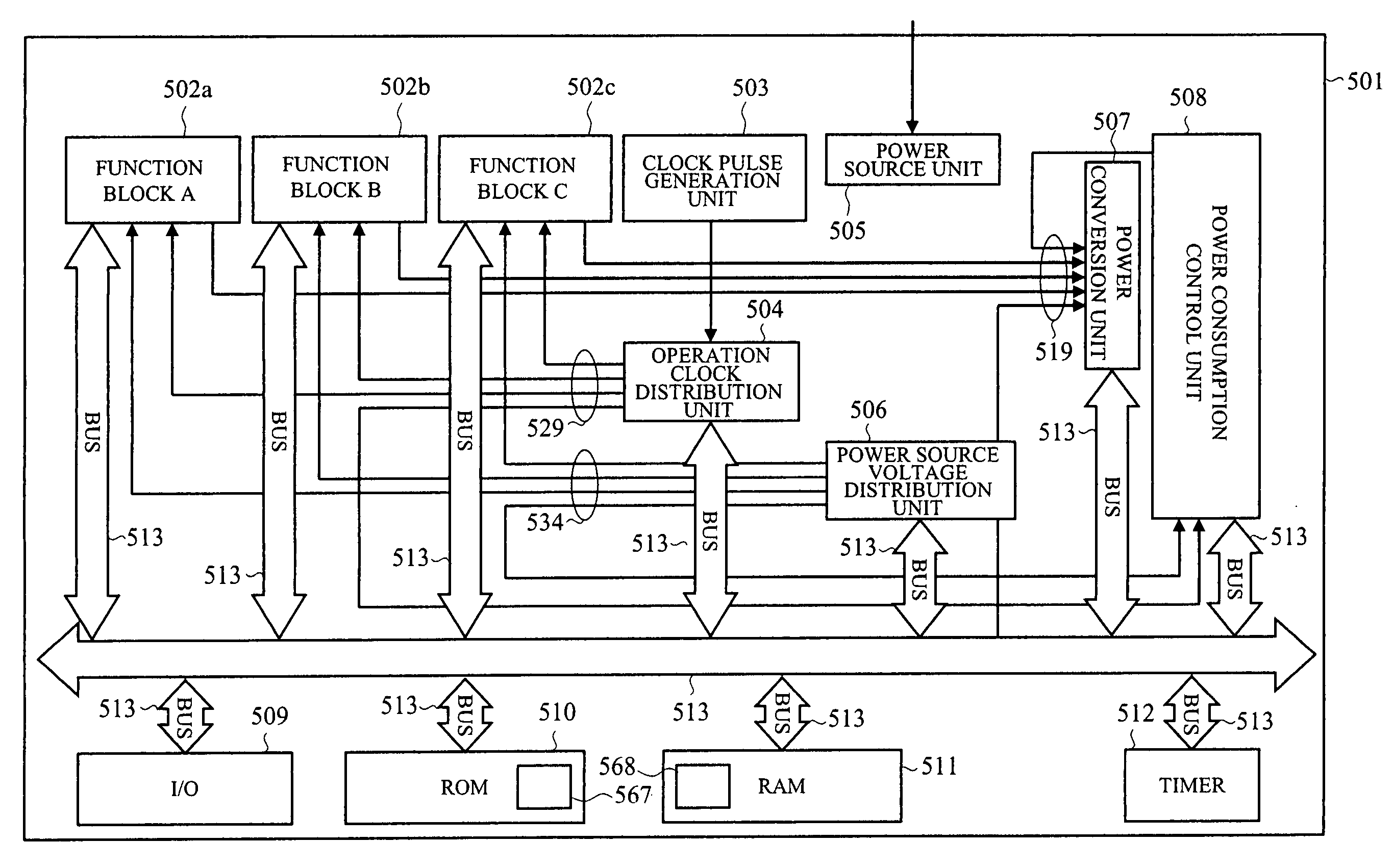
First, as the first problem, for example when the function block 111 is a processor that can flexibly change processing contents, different from ASIC where the power value can be fixed, the required power is different per processing content, that is, per task, therefore, the number of combinations of power distribution 203 is large and they become complicated, therefore it is difficult to package a power distribution candidate table unit 202, and it poses a problem.
However, as the second problem, for example, when the function block to which the power distribution unit 105 supplies low power source voltage and low operation frequency, that is, supplies low power in the course of process and satisfies a specified process to complete it, since the priority and the contents of the power distribution method are not clear, there is a fear that it cannot supply high power to the power distribution unit 105 and high speed processing cannot ever be recovered.
Further, when the total required power exceeds the power budget value in the course of process, for example, in the case where the total required power is made low to a certain function block 111 according to a priority by use of the power gating technology, since the process of the function block 111 is stopped by the power consumption control unit 401, if the power consumption control unit 401 lets the function block 111 be uncontrolled, operation cannot be made later, and there occurs a fear that the dead line of application specifications cannot be satisfied.
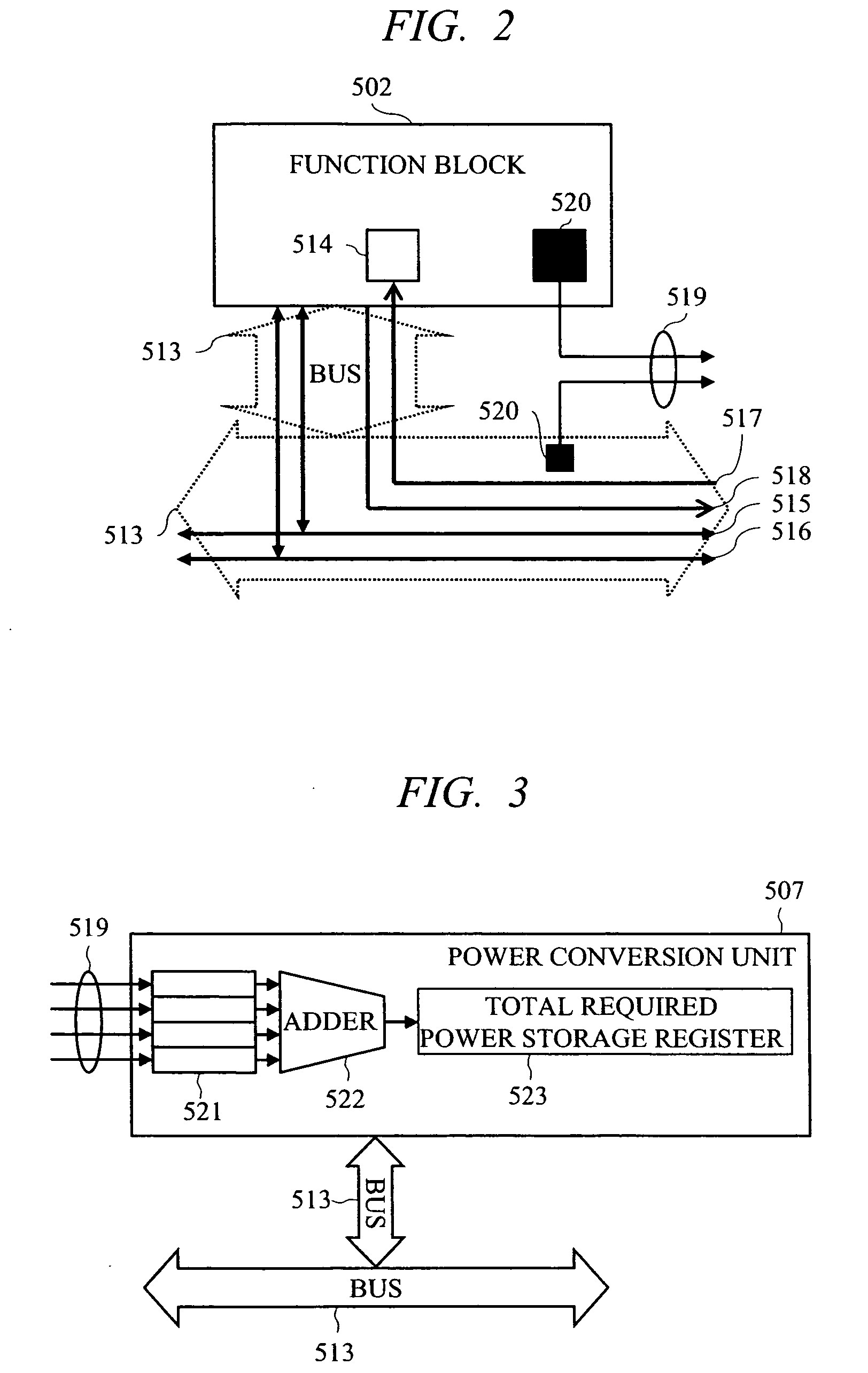
The third problem is that the power consumption of the power consumption control unit 401 is added to the total required power.
Further, the fourth problem is to limit the maximum power value of the digital LSI within the allowable power of power source IC.
When the power consumption control unit fails rapid sampling of large total required power by simultaneous driving of many function blocks, that is, when timing of comparison with the power budget value is lost, the allowable power of power source IC is exceeded, and sufficient power cannot be supplied to the respective function blocks, and the process is broken and nonconformity occurs.
The fifth problem is to judge whether the set of function blocks is in idle state or not.
The sixth problem is that even when plural function blocks 111 are loaded, it is necessary to set power in other function blocks than the power consumption control unit.

Method used


Image

  • Semiconductor integrated circuit device and power consumption control device
  • Semiconductor integrated circuit device and power consumption control device
  • Semiconductor integrated circuit device and power consumption control device

Examples


Embodiment Construction

[0088] Hereinafter, embodiments of the present invention will be described in detail with reference to the accompanying drawings. Note that components having the same function are denoted by the same reference symbols throughout the drawings for describing the embodiment, and the repetitive description thereof will be omitted.

[0089]FIG. 1 is a figure for explaining a preferred embodiment of a hardware configuration of a representative example according to the present invention.

[0090] A semiconductor integrated circuit device 501 includes a single or plural function blocks 502, a clock pulse generation unit 503, an operation clock distribution unit 504, a power source unit 505, a power source voltage distribution unit 506, a power conversion unit 507, a power consumption control unit 508, an I / O unit 509, a ROM (nonvolatile semiconductor memory) 510, a RAM (volatile semiconductor memory) 511, a timer 512, and buses 513.

[0091] The function blocks 502, the operation clock distributi...


PUM


Abstract

To perform execution scheduling of function blocks so as to control the total required power of the function blocks within a supplyable power budget value, and thereby realize stable operations at low power consumption. Function block identifiers are allotted to all the function blocks, and to a RAM area that a power consumption control device can read and write, a list to store identifiers and task priority, power mode value showing power states, and power mode time showing the holding time of power states can be linked. A single or plural link lists for controlling the schedules of tasks operating on the function blocks, a link list for controlling the function block in execution currently in high power mode, a link list for controlling the function block in stop currently in stop mode, and a link list for controlling the function block in execution currently in low power mode are allotted, and thereby the power source and the operation clock are controlled by the power consumption control device.

Description

CROSS-REFERENCE TO RELATED APPLICATION [0001] The present application claims priority from Japanese Patent Application No. JP 2005-294757 filed on Oct. 7, 2005, the content of which is hereby incorporated by reference into this application. TECHNICAL FIELD OF THE INVENTION [0002] The present invention relates to a low power consumption technology in a semiconductor integrated circuit device, more specifically to a technology effective for power consumption control in the functional block in the semiconductor integrated circuit device. BACKGROUND OF THE INVENTION [0003] In recent years, digital household electric appliances including battery-driven types such as cell phones, digital cameras, portable audio players and the like, and stationary types such as digital TV sets, digital video disk players, digital hard disk recorders and the like have become compact, thin and light-weight, and semiconductor integrated circuit devices such as digital LSI (Large Scale Integration) and the li...

Claims


Application Information

Patent Timeline
Patent Type & Authority Applications(United States)
IPC IPC(8): G06F1/00
CPCG06F1/3203G06F1/329Y02B60/144Y02B60/32Y02D10/00Y02D30/50
Inventor MISAKA, SATOSHISAEN, MAKOTOYAMADA, TETSUYATOYAMA, KEISUKEOSADA, KENICHI
Owner RENESAS ELECTRONICS CORP
Why Eureka
Try Eureka