Method of manufacturing electrical resistance heating element

a technology of heating element and resistance, which is applied in the field of manufacturing methods of electrical resistance heating elements, can solve the problems of particle development of conventional semiconductor manufacturing apparatuses, non-uniform generation of plasma, and shrinkage of molded form incident to densification, and achieve the effect of reducing the range of variations in applied pressur

Active Publication Date: 2007-10-02
NGK INSULATORS LTD
View PDF11 Cites 33 Cited by
  • Summary
  • Abstract
  • Description
  • Claims
  • Application Information

AI Technical Summary

Benefits of technology

[0017]According to the present invention, the plasma-generating electrode is formed on the sintered ceramics. This makes it possible to prevent the sintered ceramics from shrinking during sintering or from deforming due to variations in thermal conductivity in the sintered ceramics. When the sintered ceramics have a predetermined shape and the electrode is formed on the sintered ceramics, this arrangement enables disposing the electrode at a predetermined position, and also enables reducing the range of variations in the thickness of the dielectric layer.
[0031]Further, grinding takes place so that the T / A ratio falls within the above-mentioned range. This allows reducing the range of variations in applied pressure, so that the electrode can be flatly embedded.

Problems solved by technology

However, conventional semiconductor manufacturing apparatuses have a problem of particles developing.
However, the method of manufacturing the ceramic heating resistor mentioned above has the problem of shrinkage of the molded form incident to densification which occurs during sintering, because the steps of charging the ceramic powder and sintering the molded form take place after the step of disposing the winding of the high melting point metal wire on the preform.
A non-uniform thickness of the dielectric layer leads to non-uniform generation of plasma, because the intensity of plasma depends on the position at which the plasma-generating electrode is embedded, that is, the thickness of the dielectric layer.
Non-uniform generation of plasma leads to non-uniform deposition on a wafer or the like, thus to a reduction in the yield of a product such as a wafer, and thus to deterioration in quality, which is a problem of the above-mentioned method.

Method used


Image

  • Method of manufacturing electrical resistance heating element
  • Method of manufacturing electrical resistance heating element
  • Method of manufacturing electrical resistance heating element

Examples


examples 1 to 6

[Making of Sintered Ceramics]

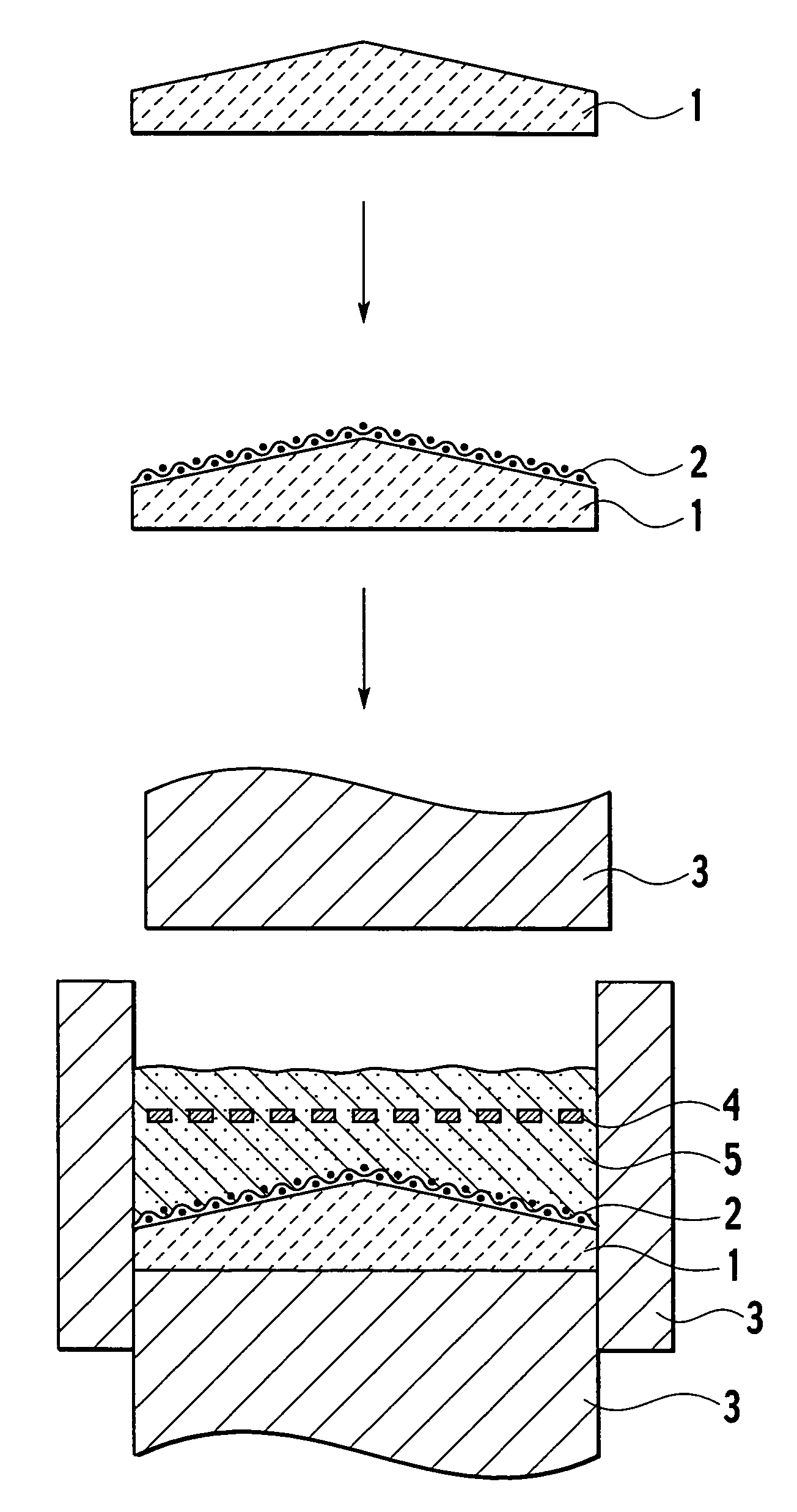
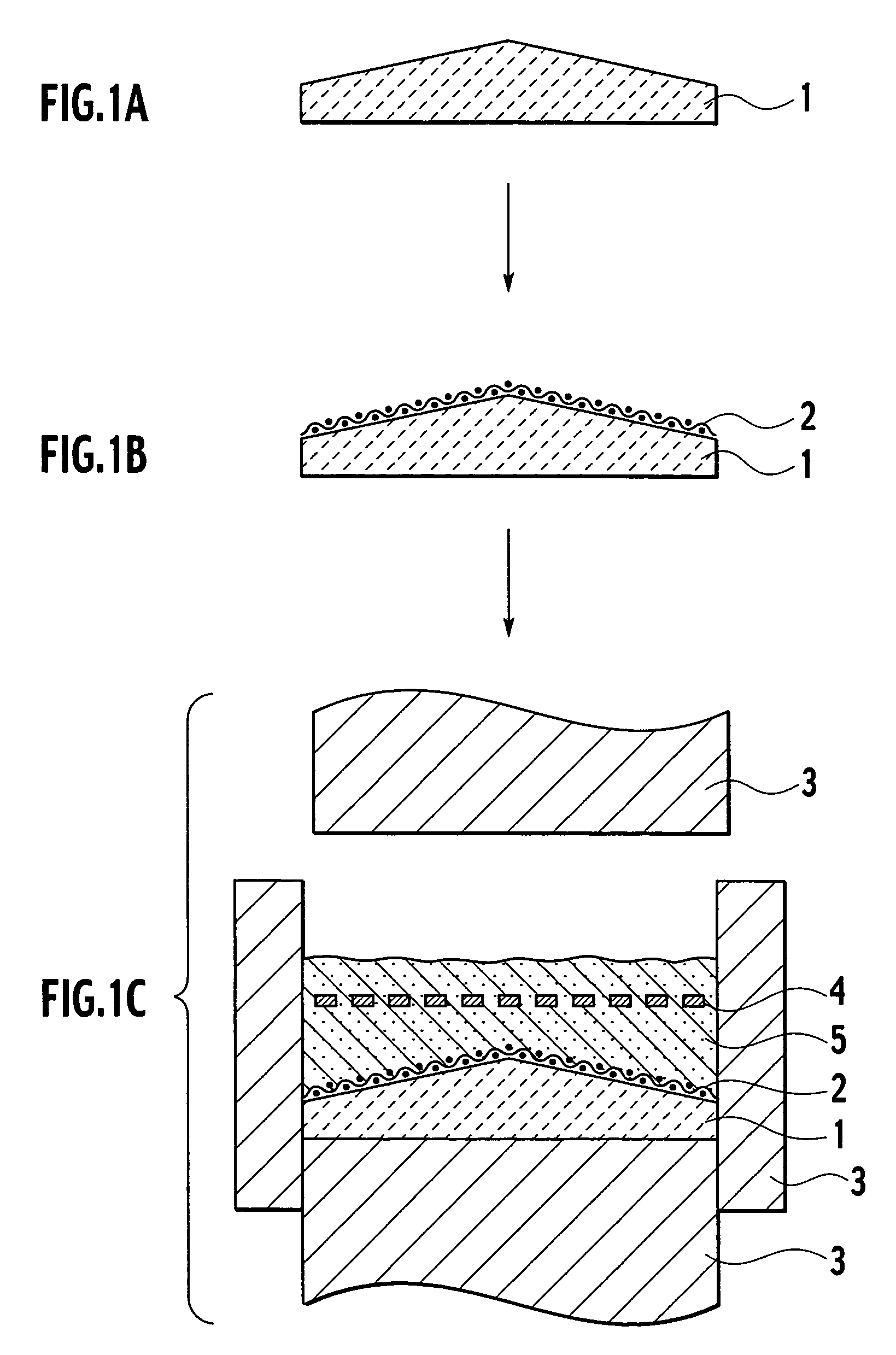
[0056]Aluminum nitride (AlN) powder containing 5% yttrium oxide (Y2O3) powder was prepared. The aluminum nitride powder containing the yttrium oxide powder was charged into a uniaxial pressing machine, and the charged powder was uniaxially pressed into a disc-shaped molded form under a pressure of 200 kg / cm2. Then, the resulting molded form was sintered into sintered ceramics having a diameter, of 340 mm and a thickness of 8 mm by hot pressing (HP) at a temperature of 1820 degrees centigrade under a pressure of 200 kg / cm2.

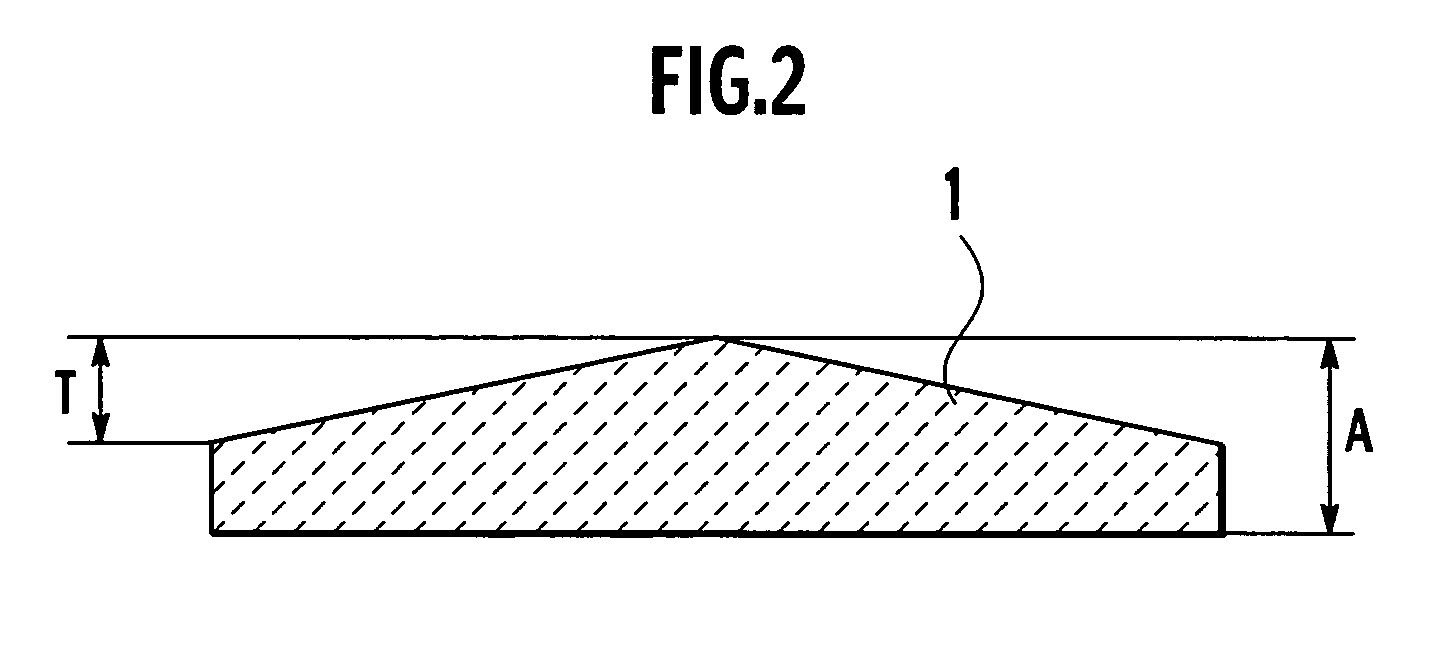
[0057]Then, the resulting disc-shaped sintered ceramics underwent rotary surface grinding. In rotary surface grinding, a diamond grinding wheel #200 was used as a grinding tool to grind the sintered ceramics into a disc shape or a conical shape, thereby forming six types of sintered ceramics. Incidentally, the conical shape means that the sintered ceramics are convex at the center on the surface on which the RF electrode is to be formed...


PUM

PropertyMeasurementUnit
thicknessaaaaaaaaaa
thicknessaaaaaaaaaa
temperatureaaaaaaaaaa

Abstract

A method of manufacturing an electrical-resistance heating element includes forming sintered ceramics or calcined ceramics, forming an electrode on the sintered ceramics or the calcined ceramics, and forming a ceramic base material having mainly a high melting point metal on the electrode embedded therein, thereby forming a heating element with built-in electrode.

Description

CROSS REFERENCE TO RELATED APPLICATION[0001]This application is based upon and claims the benefit of priority from prior U.S. Provisional Application No. 60 / 494,525, filed on Aug. 12, 2003; the entire contents of which are incorporated herein by reference.BACKGROUND OF THE INVENTION[0002]1. Field of the Invention[0003]The present invention relates to a method of manufacturing an electrical-resistance heating element, such as a heater, an electrostatic chuck, or an RF susceptor, to be applied to a semiconductor manufacturing apparatus such as a thermal CVD apparatus or an etching apparatus.[0004]2. Description of the Related Art[0005]In the field of semiconductor manufacturing technology, a wafer or the like is often subjected to processes such as plasma etching, chemical vapor deposition (CVD), and ion plating. For these processes, a heating apparatus (or a heater) is used as a component for heating the wafer, and an electrostatic chuck and an RF susceptor is used as a component for...

Claims


Application Information

Patent Timeline
Patent Type & Authority Patents(United States)
IPC IPC(8): H05B3/00H05B3/20C04B35/00H01C17/065H01C17/28H01L21/00H01L21/02H01L21/68H01L21/683H05B3/10H05B3/12H05B3/14H05B3/18H05B3/74
CPCH01C17/06513H01C17/288H01L21/67103H01L21/6831Y10T29/49124Y10T29/49158Y10T29/49098Y10T29/49163Y10T29/49087Y10T29/49083H05B3/14
Inventor MATSUDA, HIROTONOBORI, KAZUHIROMORI, YUTAKA
Owner NGK INSULATORS LTD
Why Eureka
Try Eureka