Light emitting module and lamp

a technology which is applied in the field of light emitting modules and lamps, can solve the problems of high cost and difficulty in writing a large quantity of patterns at a time, and achieve the effect of reducing the reflection of ligh

Inactive Publication Date: 2007-10-16
KOITO MFG CO LTD
View PDF10 Cites 38 Cited by
  • Summary
  • Abstract
  • Description
  • Claims
  • Application Information

AI Technical Summary

Benefits of technology

[0008]According to the first aspect of the present invention, there is provided a light-emitting module that emits light. The light-emitting module includes: a semiconductor light-emitting element that emits light; and a light transmission member that is provided to cover the semiconductor light-emitting element with materials for transmitting the light emitted from the semiconductor light-emitting element and forms a sub-wavelength grating for reducing reflection of the light on its outgoing face for sending the light incident from an interface facing the semiconductor light-emitting element to its outside in grid periods shorter than a wavelength of the light transmitted by the light transmission member.
[0022]According to the second aspect of the present invention, there is provided a lamp that emits light. The lamp includes: a light-emitting module operable to emit light; and an optical member operable to irradiate light emitted from the light-emitting module to the outside of the lamp, in which the light-emitting module includes: a semiconductor light-emitting element that emits light; and a light transmission member that is provided to cover the semiconductor light-emitting element with materials for transmitting the light emitted from the semiconductor light-emitting element and forms a sub-wavelength grating for reducing reflection of the light on its outgoing face for sending the light incident from an interface facing the semiconductor light-emitting element to its outside in grid periods shorter than a wavelength of the light transmitted by the light transmission member, and the optical member has optical center on the semiconductor light-emitting element.

Problems solved by technology

However, in an exposure process performed by the electron beam lithography method, it is difficult to write a large quantity of patterns at a time in some cases.
Therefore, a high cost was conventionally required in some cases when desiring to produce a semiconductor light-emitting element having high light-emitting efficiency.

Method used


Image

  • Light emitting module and lamp
  • Light emitting module and lamp
  • Light emitting module and lamp

Examples


Embodiment Construction

[0041]The invention will now be described based on the preferred embodiments, which do not intend to limit the scope of the present invention, but exemplify the invention. All of the features and the combinations thereof described in the embodiment are not necessarily essential to the invention.

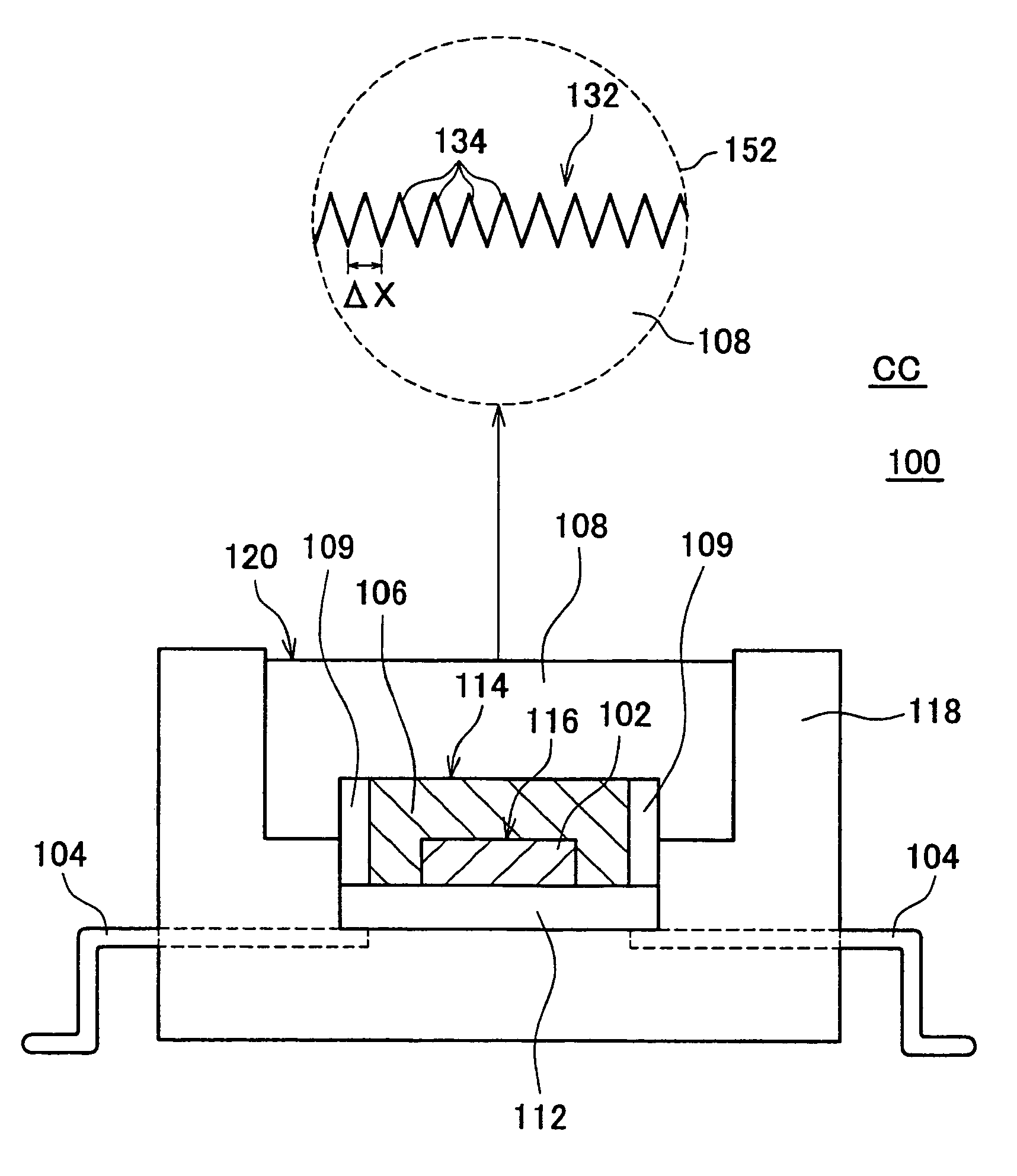
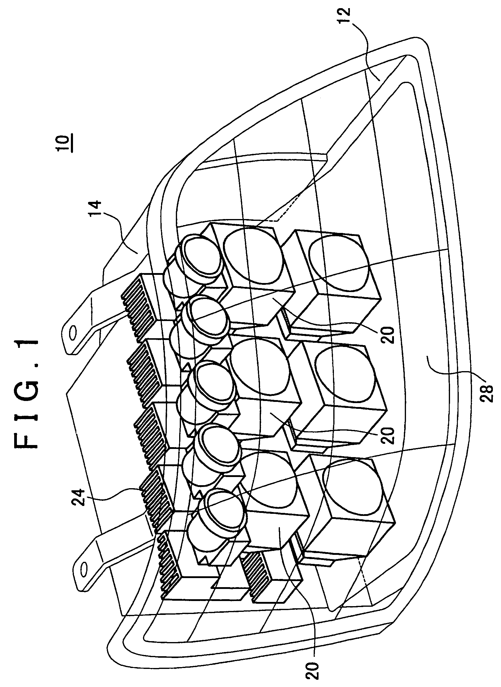
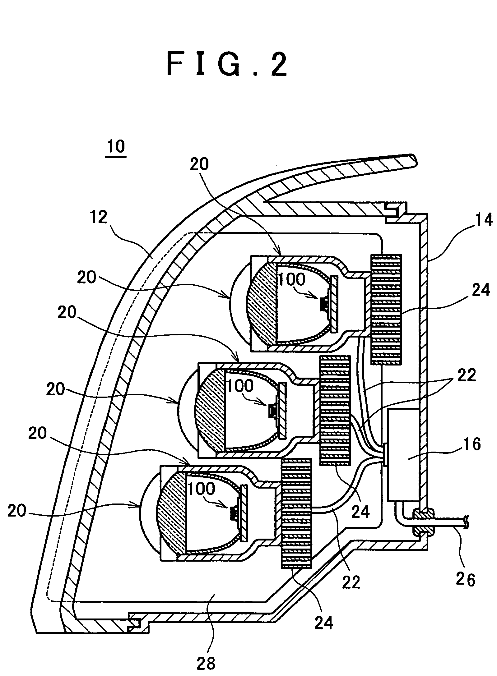
[0042]FIGS. 1 and 2 are views exemplary showing a configuration of a vehicular lamp 10 according to an embodiment of the present invention. FIG. 1 is a perspective view of the vehicular lamp 10. FIG. 2 is a horizontal sectional view of the vehicular lamp 10 by a horizontal plane crossing a light source unit 20 in the middle stage. The object of the present example is to provide an LED module 100 at low cost, which is adapted to form a light distribution pattern with high precision. The vehicular lamp 10 is, e.g., a headlight (a head lamp) used for a vehicle such as an automobile, and irradiates light ahead of the vehicle. The vehicular lamp 10 includes a plurality of light source units 20, a ...


PUM


Abstract

A light-emitting module having a light-emitting efficiency. The light-emitting module that emits light includes a semiconductor light-emitting element that emits light; and a light transmission member that is provided to cover the semiconductor light-emitting element with materials for transmitting the light emitted from the semiconductor light-emitting element and forms a sub-wavelength grating for reducing reflection of the light on its outgoing face for sending the light incident from an interface facing said semiconductor light-emitting element to its outside in grid periods shorter than a wavelength of the light transmitted by the light transmission member.

Description

[0001]This patent application claims priority from a Japanese Patent Application No. 2004-013124 filed on Jan. 21, 2004, the contents of which are incorporated herein by reference.BACKGROUND OF THE INVENTION[0002]1. Field of the Invention[0003]The present invention relates to a light-emitting module and a lamp.[0004]2. Description of Related Art[0005]A light-emitting module such as a light-emitting diode utilizes a semiconductor light-emitting element that emits light. Recently, the configuration capable of improving light-emitting efficiency by providing a plurality of convex portions on the surface of the semiconductor light-emitting element is known as disclosed, for example, in Japanese Patent Laid-Open No. 2003-86835 (pages 1-6, FIGS. 1-13). The plurality of convex portions is arranged in the shape of grid in shorter periods than light wavelength. In addition, the plurality of convex portions is formed by etching the surface of the semiconductor light-emitting element. For this...

Claims


Application Information

Patent Timeline
Patent Type & Authority Patents(United States)
IPC IPC(8): H01L33/00G02B5/18F21S2/00F21S8/10F21S8/12F21V5/04F21W101/10F21Y101/02H01L29/06H01L33/32H01L33/50H01L33/54H01L33/56H01L33/60H01L33/62H01L33/64H05B33/20
CPCF21S48/1154F21S48/1163H01L2933/0091F21Y2113/00H01L33/56F21Y2101/02F21Y2115/10F21S41/143F21S41/155
Inventor TAKEDA, HITOSHIDAICHOU, HISAYOSHITOKIDA, TSUKASAISHIDA, HIROYUKI
Owner KOITO MFG CO LTD
Why Eureka
Try Eureka