System and method for verifying signal propagation delays of circuit traces of a PCB layout

Inactive Publication Date: 2007-10-16
HONG FU JIN PRECISION IND (SHENZHEN) CO LTD +1
View PDF10 Cites 5 Cited by
  • Summary
  • Abstract
  • Description
  • Claims
  • Application Information

AI Technical Summary

Benefits of technology

[0009]A main objective of the present invention is to provide a system and method which can

Problems solved by technology

Even more that previously, high-speed, high-frequency signals being driven between chips via traces on a PCB are liable to detrimental impedance effects.
One manifestation of these impedance effects is unwanted reflections due to impedance mismatches.
The high-speed, high-frequency signals may also be prone to cross-talk and electromagnetic interference (EMI).
EMI is an electrical disturbance in an electronics-based system.
In particu

Method used


Image

  • System and method for verifying signal propagation delays of circuit traces of a PCB layout
  • System and method for verifying signal propagation delays of circuit traces of a PCB layout
  • System and method for verifying signal propagation delays of circuit traces of a PCB layout

Examples


Embodiment Construction

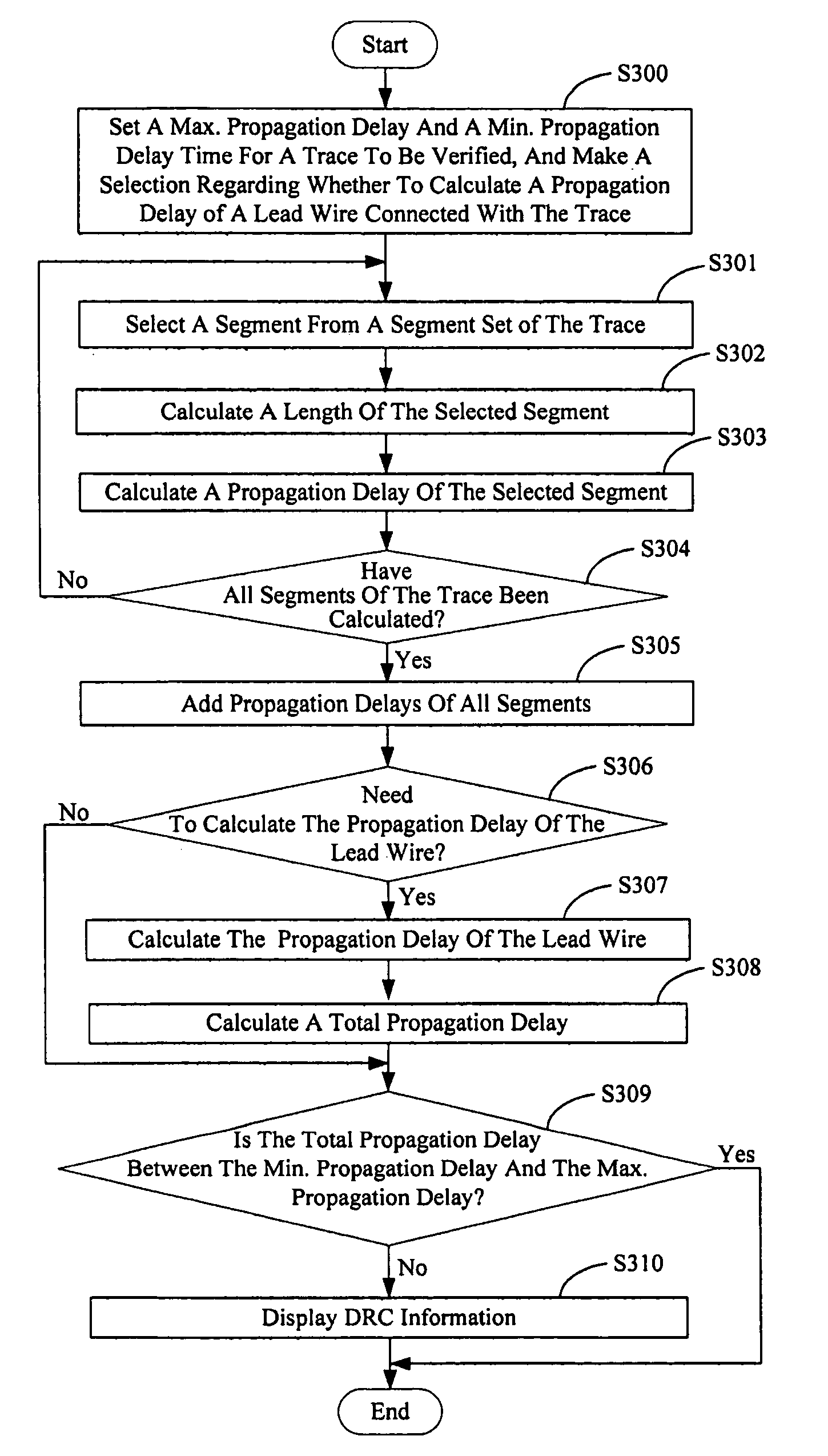
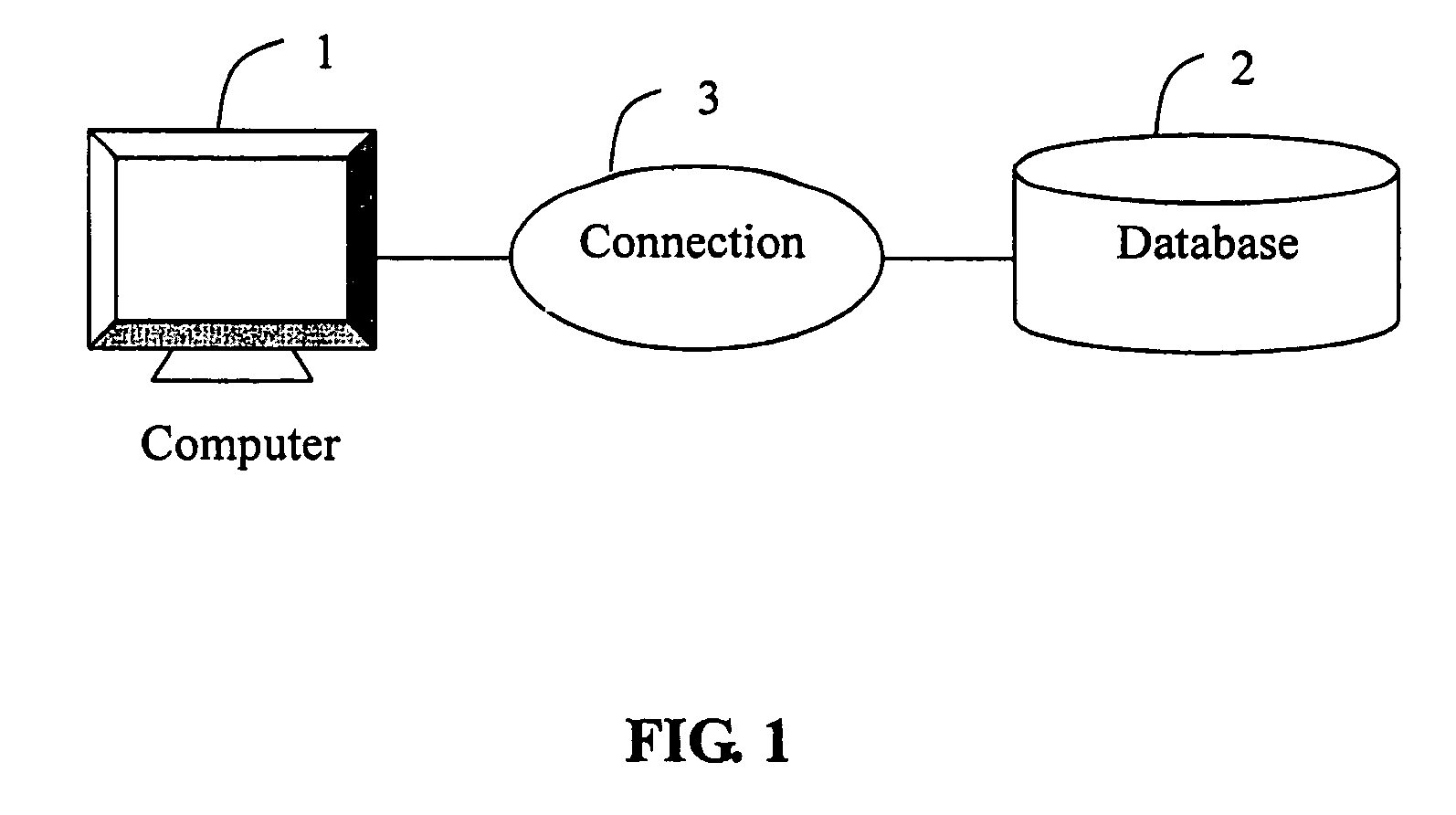
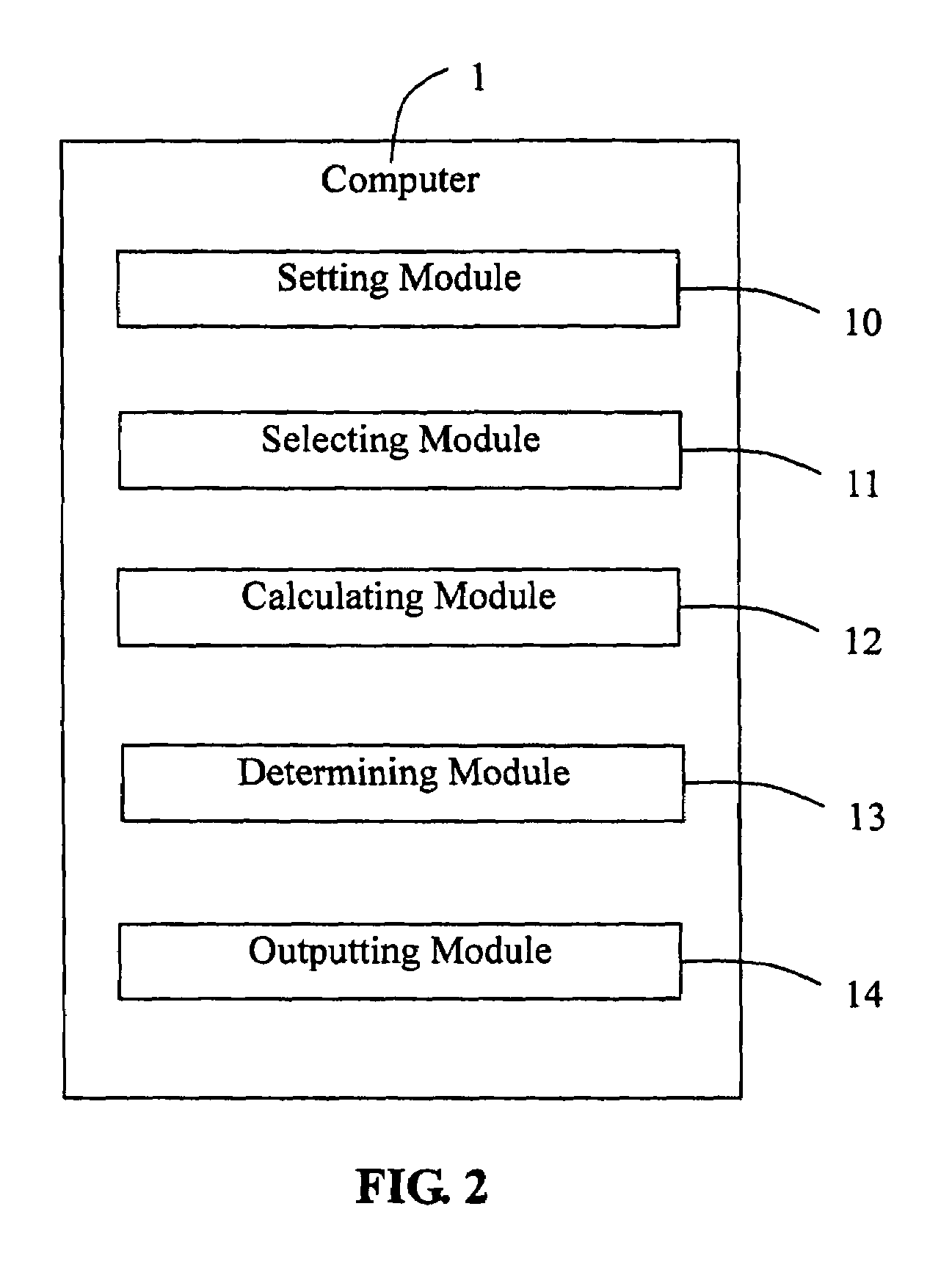
[0017]FIG. 1 is a schematic diagram of hardware infrastructure of a system for verifying signal propagation delays of circuit traces of a printed circuit board (PCB) layout (hereinafter, “the system”) in accordance with the preferred embodiment of the present invention. The system comprises a computer 1, a database 2, and a connection 3. The computer 1 contains a plurality of function modules installed therein (described in detail below in relation to FIG. 2). The computer 1 calculates and verifies a signal propagation delay of each trace of the PCB in order to determine whether the PCB layout is satisfactory. Generally, there are a plurality of traces in the PCB. Each trace includes a plurality of segments, which can be included in a segment set. That is, each trace corresponds to a segment set. Electronic components are set on the PCB. Such electronic components comprise chip devices, a central processing unit (CPU), one or more memories, etc. The electronic components can be enca...


PUM


Abstract

A system for verifying signal propagation delays of circuit traces of a printed circuit board (PCB) layout includes a computer (1). The computer includes: a setting module (10) for setting a minimum propagation delay and a maximum propagation delay for a trace to be verified, and making a selection regarding whether to calculate a propagation delay of a lead wire connected with the trace; a selecting module (11) for selecting a segment from a segment set of the trace; a calculating module (12) for calculating a propagation delay of the segment, the trace and the lead wire, and a total propagation delay; and a determining module (13) for determining whether all segments of the trace have been calculated, and whether the total propagation delay is between the minimum propagation delay and the maximum propagation delay. A related method is also disclosed.

Description

BACKGROUND OF THE INVENTION[0001]1. Field of the Invention[0002]The present invention relates to systems and methods of verifying signal propagation delays in electronic equipment, and particularly to a system and method for verifying propagation delays of circuit traces of a printed circuit board (PCB) layout.[0003]2. Related Art of the Invention[0004]A PCB of a typical computer connects chip devices together, and also connects the chip devices to external components such as a keyboard and storage devices. The PCB generally utilizes circuit traces thereof to fulfill the connections. Some chip devices have multiple traces that send and / or receive data bits substantially simultaneously. The time that it takes for data to traverse a trace is known as propagation delay.[0005]Computer chip sizes are continuing to be miniaturized, and electrical signals are being clocked at ever increasing frequencies. Even more that previously, high-speed, high-frequency signals being driven between chi...

Claims


Application Information

Patent Timeline
IPC IPC(8): G06F9/45G06F9/455H03H11/26G06F17/50
CPCG06F17/5022G06F30/33
Inventor TSAI, HUNG-YUANTONG, MO-YING
Owner HONG FU JIN PRECISION IND (SHENZHEN) CO LTD
Why Eureka
Try Eureka