Method and apparatus for network with multilayer metalization

a multi-layer metalization and network technology, applied in data switching networks, data switching networks, architectures with multiple processing units, etc., can solve the problems of not being able to evenly spread wires across all channels without increasing channel widths, superlinear growth of switching requirements with an increase in the number of compute blocks, and hierarchical scheme not eliminating asymptotic switch requirements. , to achieve the effect of fast and guaranteed routing

US7285487B2Inactive Publication Date: 2007-10-23CALIFORNIA INST OF TECH
32 Cites 22 Cited by

Patent Information

Authority / Receiving Office
US · United States
Patent Type
Patents(United States)
Current Assignee / Owner
Publication Date
2007-10-23
Estimated Expiration
Not applicable · inactive patent

Smart Images

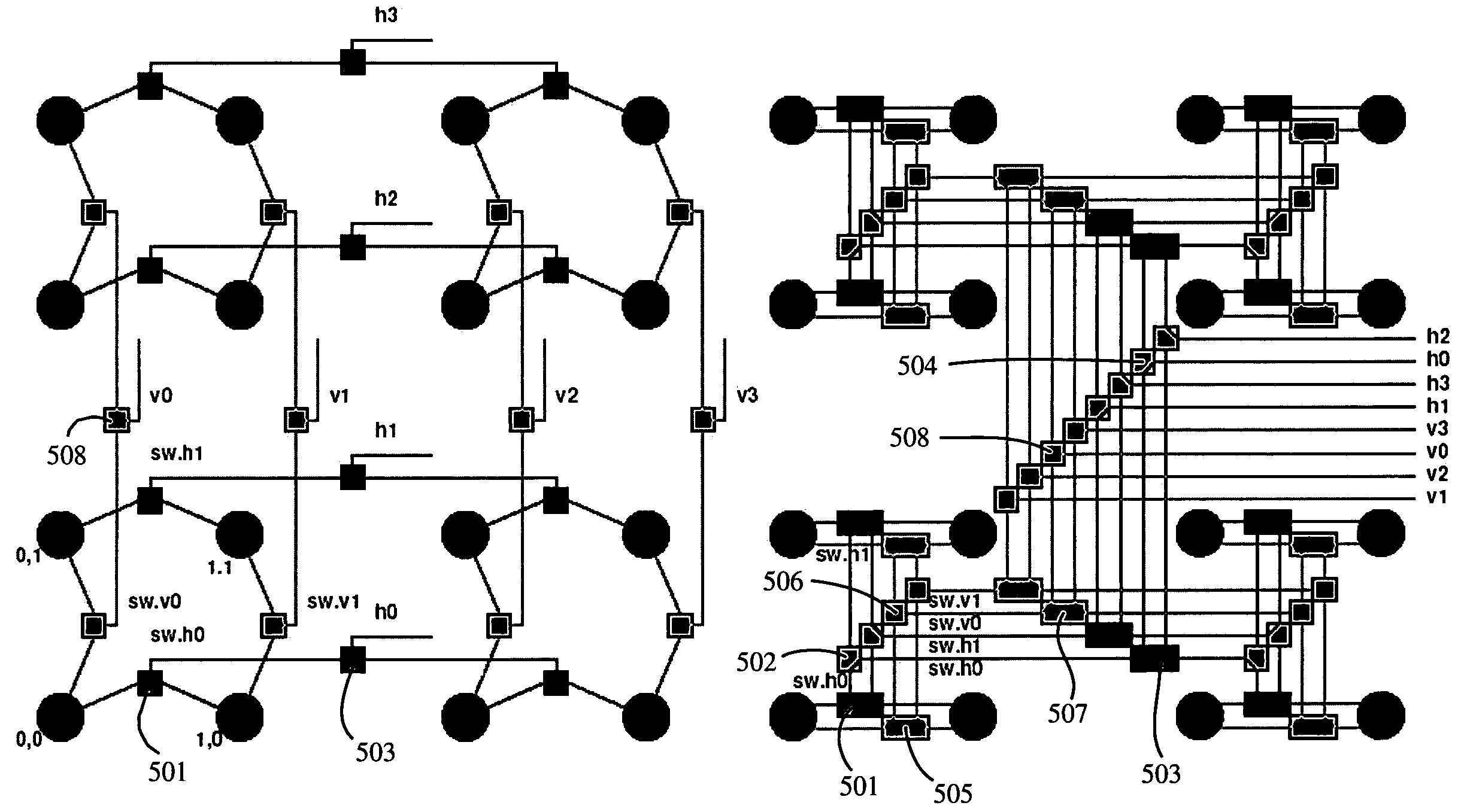
  • Figure 1
    Figure 1
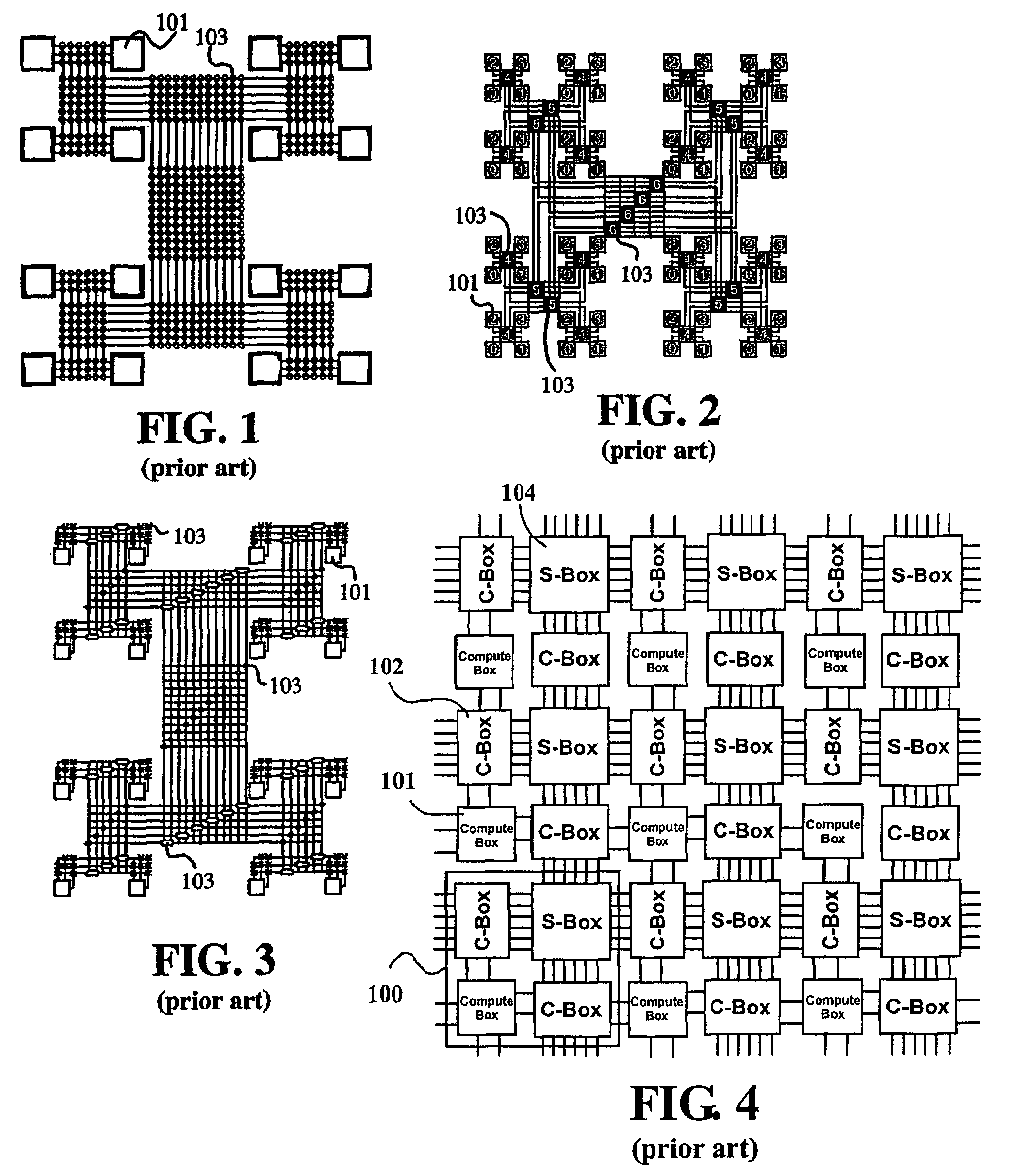
  • Figure 2
    Figure 2
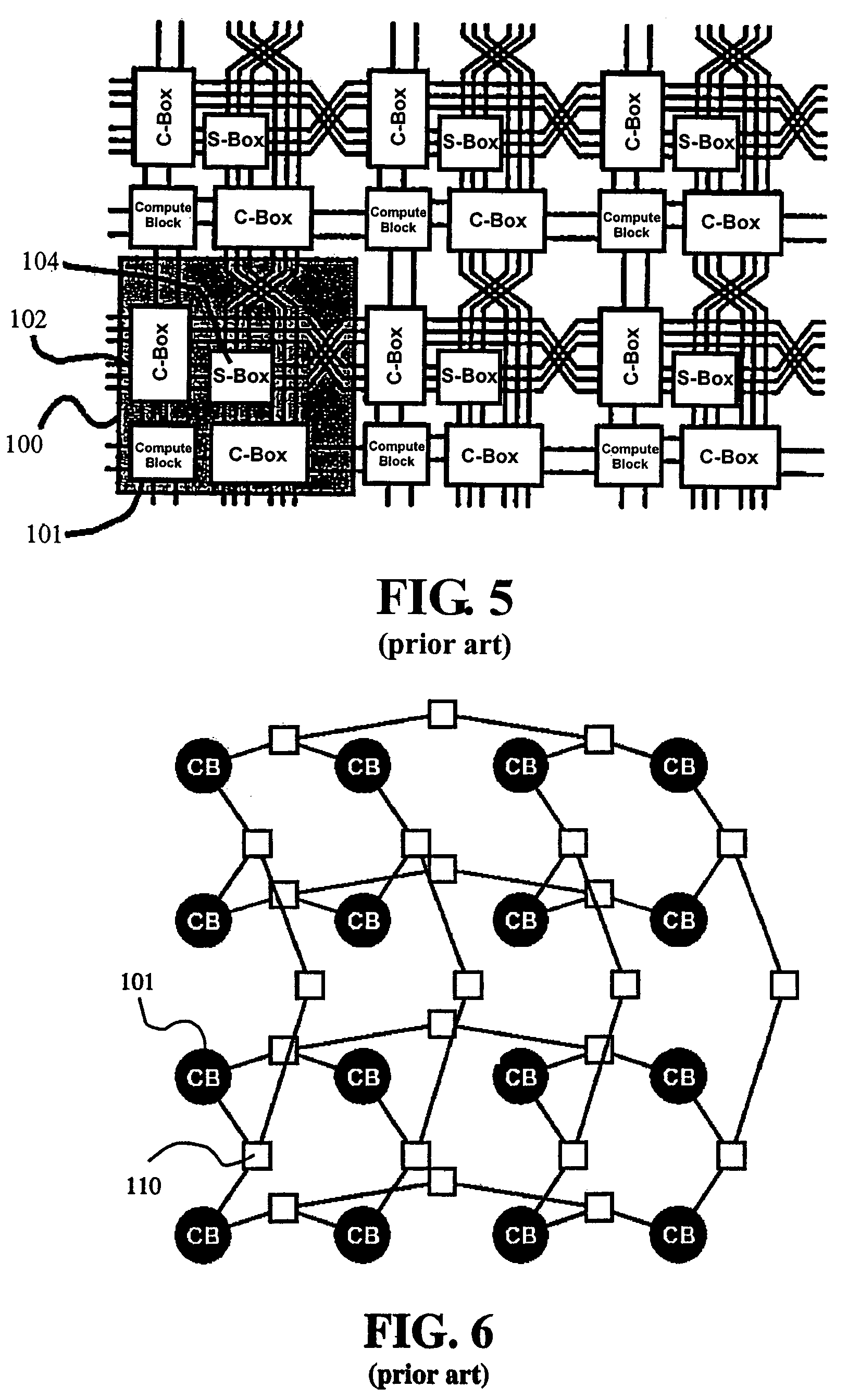
  • Figure 3
    Figure 3
Patent Text Reader

Abstract

A network for interconnecting processing element nodes which supports rich interconnection while having a number of switching elements which is linear in the number of processing elements interconnected. Processing elements connect to the lowest level of the tree and the higher levels of the tree make connections between the processing elements. The processing elements may be laid out in a two dimensional grid and one or more horizontal and vertical trees may be used to connect between the processing elements with corner switches used to connect between the horizontal and vertical trees. The levels of the tree can be accommodated in multiple layers of metalization such that the entire layout requires a two-dimensional area which is linear in the number of processing elements supported.
Need to check novelty before this filing date? Find Prior Art

Description

CROSS REFERENCE TO RELATED APPLICATIONS

[0001] This application claims benefit of the following applications: U.S. Provisional Application No. 60 / 490,213, filed on Jul. 24, 2003; U.S. Provisional Application No. 60 / 498,811, filed on Aug. 29, 2003; and U.S. Provisional Application No. 60 / 502,539, filed on Sep. 12, 2003, all of which are incorporated herein by reference in their entirety.STATEMENT REGARDING FEDERALLY SPONSORED RESEARCH OR DEVELOPMENT

[0002] The present invention was made with support from the United States Government under Grant No. N00014-01-0651 awarded by the Office of Navel Research of the Department of the Navy. The United States Government has certain rights in the invention.BACKGROUND

[0003] 1. Field

[0004] The present disclosure describes methods and techniques for interconnecting a collection of processing elements in which multiple metallization layers may be used. For example, the present disclosure describes a method and apparatus for interconnecting compute, memo...

Examples

Embodiment Construction

[0093]The present invention will now be described more fully hereinafter with reference to the accompanying drawings, in which preferred embodiments of the invention are shown. This invention may be embodied in many different forms and should not be construed as limited to the embodiments set forth herein. Further, the dimensions of layers and other elements shown in the accompanying drawings may be exaggerated to more clearly show details. The present invention should not be construed as being limited to the dimensional relations shown in the drawings, nor should the individual elements shown in the drawings be construed to be limited to the dimensions shown.

[0094]The asymptotic analysis presented above in regard to the Manhattan interconnection scheme indicates that it is necessary to bound the compute block connections to a constant if the total switches per compute block is to be contained to a constant independent of design size. Certain embodiments according to the present inv...