Integration of an amorphous silicon resistive switching device

a resistive switching and amorphous silicon technology, applied in the direction of semiconductor devices, basic electric elements, electrical apparatus, etc., can solve the problems of increasing power dissipation, non-scaling of sub-threshold slopes, and reducing device performan

Inactive Publication Date: 2012-03-29
CROSSBAR INC
View PDF20 Cites 77 Cited by
  • Summary
  • Abstract
  • Description
  • Claims
  • Application Information

AI Technical Summary

Benefits of technology

[0011]Many benefits can be achieved by ways of the present invention over convention techniques. For example, embodiments according to the present invention provide a device structure for a one transistor one resistor (1T1R) implementation. Depending on the embodiment, the transistor can be used as a select transistor for the switching device. In other embodiment, the transistor provides for a variable resistor coupled to the resistive switching device, allowing programming (for example, write, read, or erase) of the switching device at selected voltage to enable a multi bit storage capability for the resistive switching device. The variable resistance of the transistor can further control current flows to protect the resistive switching device. In other embodiments, the present invention provides a device structure and a method to form an one time programmable storage device having a stable data storage and excellent scalability.

Problems solved by technology

However, as field effect transistors (FET) approach sizes less than 100 nm, problems such as the short channel effect degrade device performance.
Moreover, such sub 100 nm device size can lead to sub-threshold slope non-scaling and also increases power dissipation.
These devices often require new materials and device structures to couple with silicon-based devices to form a memory cell, which lack one or more key attributes.
For example, Fe-RAM and MRAM devices have fast switching characteristics and good programming endurance, but their fabrication is not CMOS compatible and size is usually large.
Switching for a PCRAM device requires large amounts of power.
Organic RAM is incompatible with large volume silicon-based fabrication and device reliability is usually poor.

Method used


Image

  • Integration of an amorphous silicon resistive switching device
  • Integration of an amorphous silicon resistive switching device
  • Integration of an amorphous silicon resistive switching device

Examples


Embodiment Construction

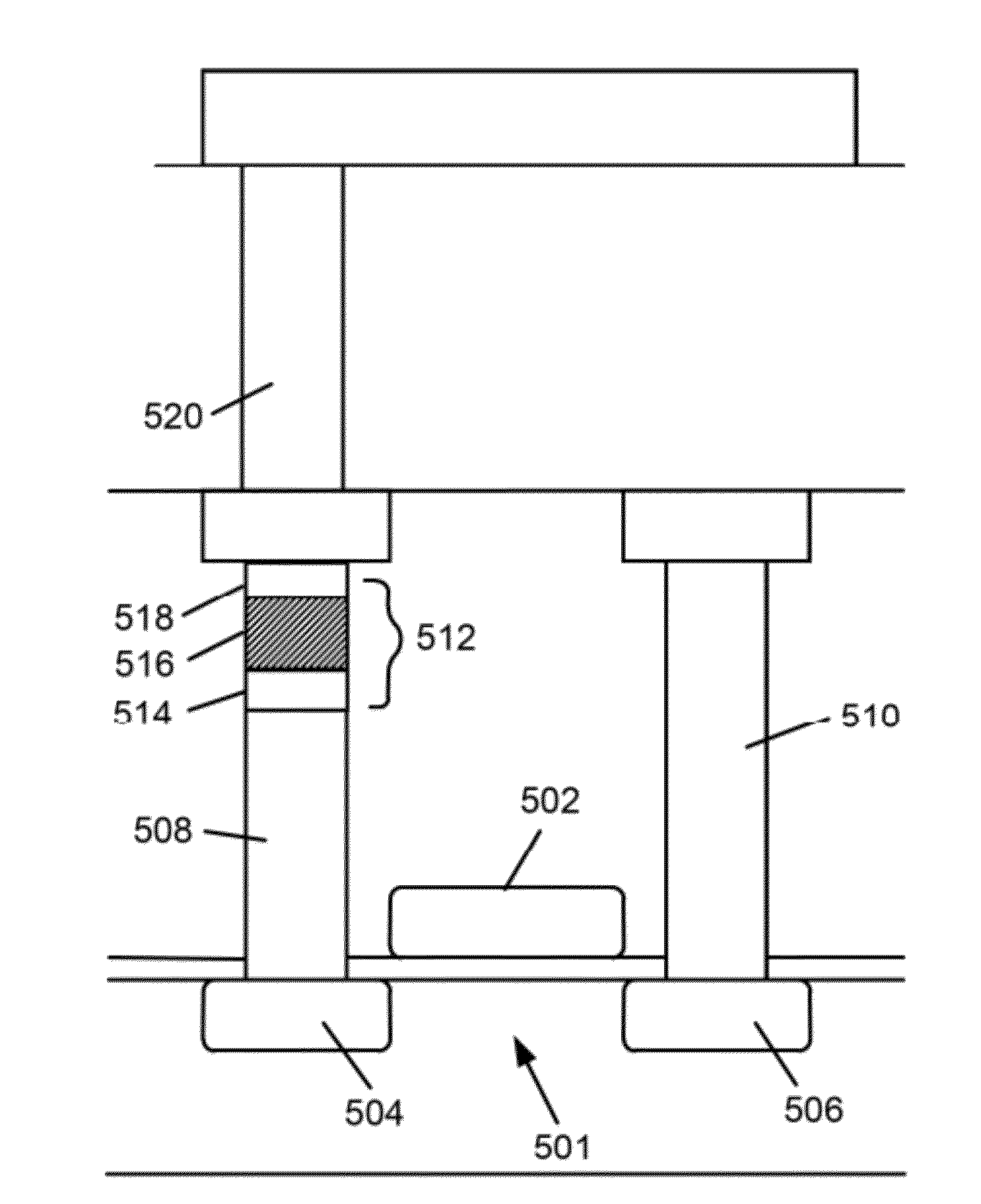
[0022]The present invention is generally related to resistive switching devices. More particularly, embodiments according to the present invention provide a method and a structure for integrating a resistive switching device with a transistor for switching control. The present invention can be applied to non-volatile resistive switching memory device. But it should be recognized that the present invention can have a much broader range of applicability.

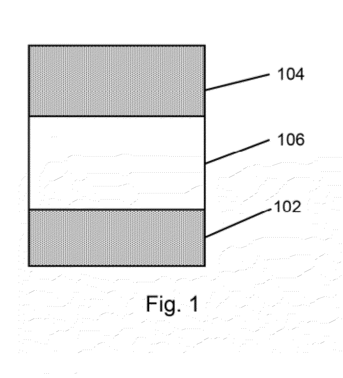
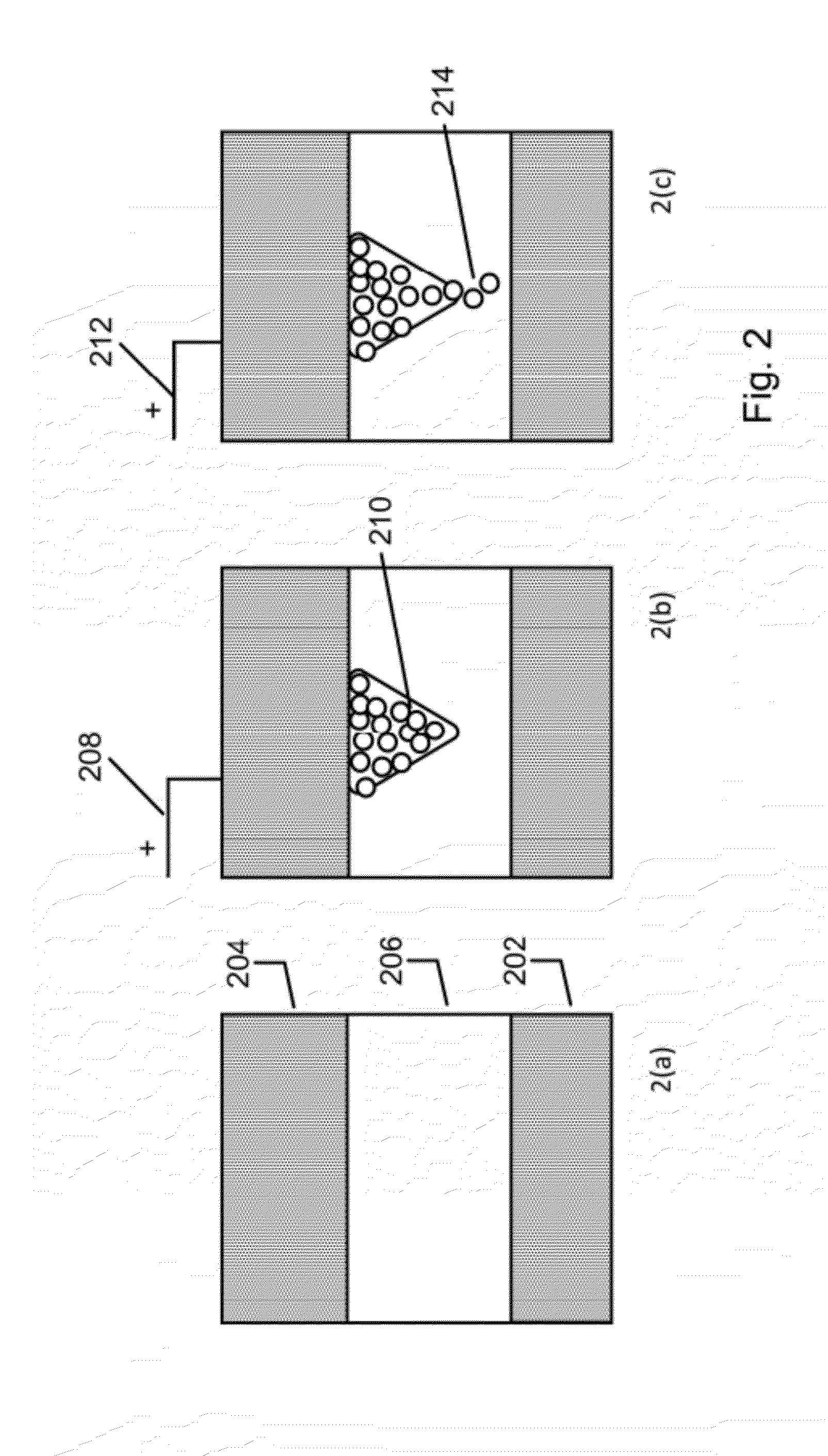
[0023]FIG. 1 is a simplified diagram illustrating a resistive switching device according to an embodiment of the present invention. As shown, the resistive switching device includes a first electrode 102, a second electrode 104, and a switching material 106 sandwiched between the top electrode and the bottom electrode. The switching material is configured to change in resistance when a voltage is applied to the first electrode or the second electrode. The first electrode and the bottom electrode can include one or more conductive mater...


PUM


Abstract

An integrated circuit device. The integrated circuit device includes a semiconductor substrate having a surface region. A gate dielectric layer overlies the surface region of the substrate. The device includes a MOS device having a p+ active region. The p+ active region forms a first electrode for a resistive switching device. The resistive switching device includes an amorphous silicon switching material overlying the p+ active region and a metal electrode overlies the first metal conductor structure. The metal electrode includes a metal material, upon application of a positive bias to the metal electrode, forms a metal region in the amorphous silicon switching material. The MOS device provides for a select transistor for the integrated circuit device.

Description

CROSS REFERENCE TO RELATED APPLICATIONS[0001]Not ApplicableSTATEMENT RELATED TO FEDERAL OR GOVERNMENT SPONSORED RESEARCH[0002]Not ApplicableBACKGROUND[0003]The present invention is generally related to resistive switching devices. More particularly, embodiments according to the present invention provide a method and a structure for integrating a resistive switching device with a transistor for switching control. The present invention can be applied to non-volatile resistive switching memory device. But it should be recognized that the present invention can have a much broader range of applicability.[0004]The success of semiconductor devices has been mainly driven by an intensive transistor down-scaling process. However, as field effect transistors (FET) approach sizes less than 100 nm, problems such as the short channel effect degrade device performance. Moreover, such sub 100 nm device size can lead to sub-threshold slope non-scaling and also increases power dissipation. It is gene...

Claims


Application Information

Patent Timeline
Patent Type & Authority Applications(United States)
IPC IPC(8): H01L27/105H01L21/8239
CPCH01L45/085H01L45/1233H01L45/1266H01L27/2436H01L45/1616H01L45/1675H01L45/1683H01L45/148H10B63/30H10N70/245H10N70/8416H10N70/826H10N70/884H10N70/023H10N70/066H10N70/063
Inventor JO, SUNG HYUNNAZARIAN, HAGOP
Owner CROSSBAR INC
Why Eureka
Try Eureka