[0007]A primary objective of the present invention is to provide a
power efficient FHSS (Frequency Hopping Spreading Spectrum) base-band
hardware architecture with characteristics of higher performance and ability of system-wide calculation in lower
power consumption, precise synchronization of system clock to reduce jitter variance of FHSS system less than three clocks of highest system clock and wider communication range under same RF condition of transmission power and receiving sensitivity.
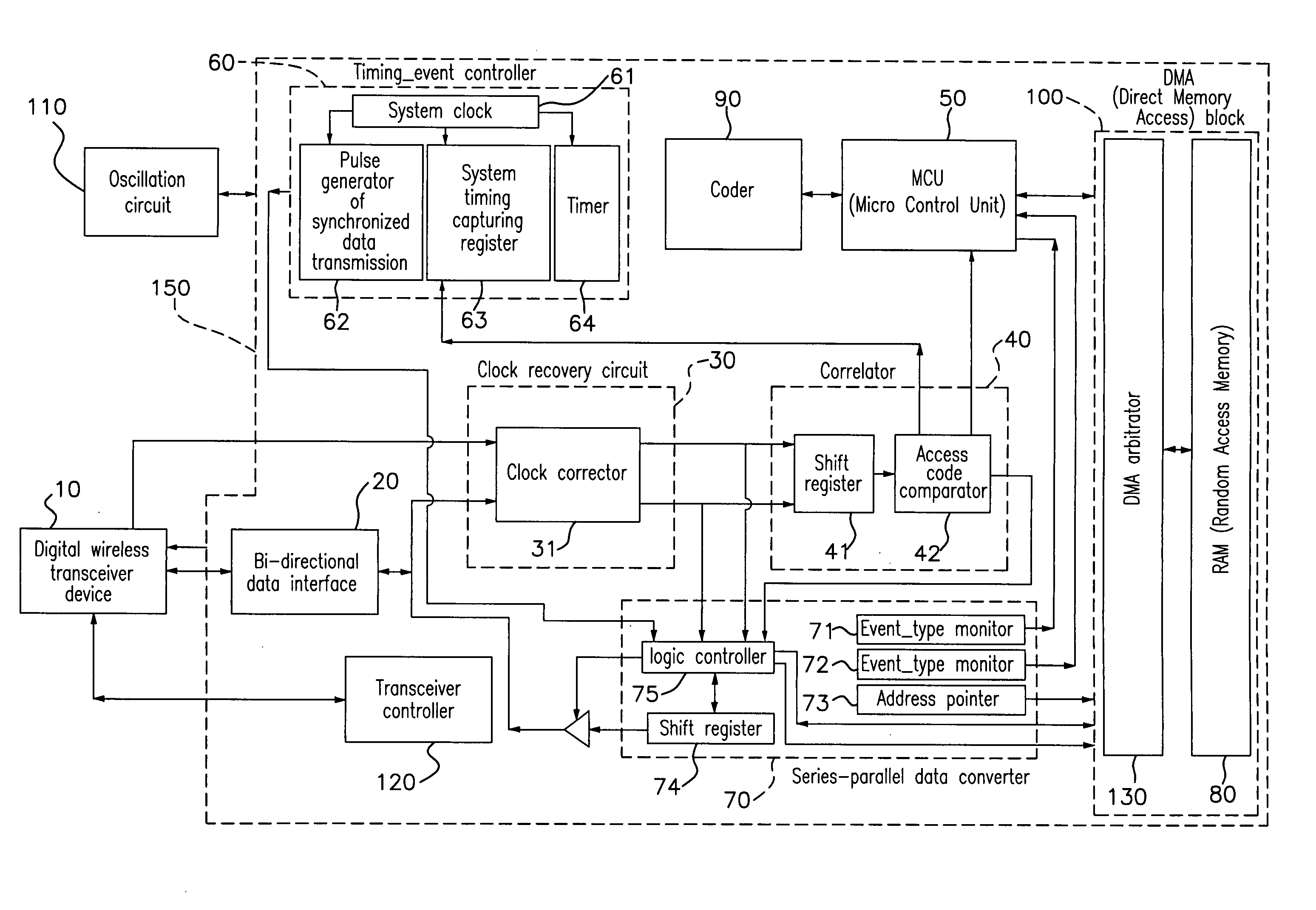
[0008]The invention comprise a digital
wireless transceiver device, a bi-directional
data interface, a
clock recovery circuit (comprising a clock corrector), a correlator (comprising a
shift register and an access code
comparator), a MCU (Micro
Control Unit), a coder, a timing_event controller (comprising a system clock, a
timer, a system timing capturing register and a
pulse generator for synchronized
data transmission), a series-parallel data converter (comprising two event_type monitors, a address pointer, a logic controller and a
shift register), a DMA (
Direct Memory Access) block (comprising a DMA arbitrator and a RAM (
Random Access Memory)), a
transceiver controller and an oscillation circuit. The
clock recovery circuit connecting to the bi-directional data interface extracts frequency and phase being carried within received data, thereby utilizing the recovered clock to latch received data in secure phase locally. The correlator calculates similarity between shifted-in received data from peer and a pre-configured local access address. An Access_
Sync signal is generated when the matching level of similar pattern exceeds preset condition. An Access_
Sync signal is passed to the MCU and the timing_event controller as an interruption signal simultaneously. Thereby, by capturing that event-triggered timing of interruption in an
automatic control circuit, it reduces jitter of reference point of system clock to a secure scale. This is the major
advantage superior to generic instruction driven by
software method. A RX_TRIG signal is also generated to notify the series-parallel data converter to launch bulk data collection, every 8-bit data is stored into RAM repeatedly without intervention from MCU. This method is another main
advantage better than the MCU of prior art which moves data by frequent routine of interruption. The MCU handles data movement between RAM in DMA block and FHSS function related blocks of this invented hardware architecture in such a specified procedure. At receive mode, the timing_event controller receives the Access_Sync interruption signal from the correlator, and system timing capturing register accepts that timing information at the moment of Interruption as a reference to adjusts local timing. As the hardware architecture can lock interruption signal quite precisely, normally, the
timing error of jitter can be lowered to less than three highest system clocks, and it can maintain a more stable wireless
digital data link to peer party. Eventually, the performance of data communication of the entire
wireless network is improved. The buffering logic controller periodically preempts MCU to DMA arbitrator for storing received data. Such combination of
control logic increases overall practicability of the present invention.
[0009]Another objective of the present invention is to provide a power efficient FHSS base-band hardware architecture, wherein the series-parallel data converter is configured with two event_type monitors, used to respectively produce a Wake_Int and a Wrap_Int interruption signals, and a address pointer to produce an address index assigned in RAM (Random-Access Memory). The series-parallel data converter and the MCU are also connected to DMA arbitrator and a shared RAM. The DMA arbitrator maintains a specific procedure to access RAM block. The series-parallel data converter, different from the prior art to process data to RAM via the MCU, sends every 8-bit data into the RAM directly without intervention of MCU. Thus, MCU can stay in
sleep mode longer. Address pointer serves as a pointer to access RAM block by increasing one integer value of address assigned automatically every time a
byte is stored. When address pointer reaches the pre-defined address, depending on actual demand and normal in middle of
payload, a Wake_Int is triggered to wake CPU up from
sleep mode, and process data in the highest clock to implement one-time bulk FEC
processing on the already received data through a parallel
bus linked to the RAM. After finishing jobs, MCU may or may not sleep and it's depended on received data progress status. As
packet payload receiving comes to the end, a Wrap_Int is triggered and attempts to wake MCU up and deactivate series-parallel data converter. Finally, MCU processes data at the highest clock speed to implement one-time bulk FEC (
Forward Error Correction)
processing upon the data received and stored. Thereby it substantially increases
processing efficiency of the MCU, and thus it has more time to
handle other digital
voice data,
digital signal processing, arithmetic operations or other applications.
[0010]Another objective of the present invention is to provide the power efficient FHSS base-band hardware architecture with the bi-directional data interface that is connected to the clock
recovery circuit, and is to use the recovered clock to take sampling from received data bit by bit in a secure window, and thus it provides a more reliable timing relation and
data integrity between peer systems.
[0011]Yet another objective of the present inventions is to provide the power efficient FHSS base-band hardware architecture, wherein the coder circuit which operates reverse function of both encoding (transmission) and decoding (receiving) to work with MCU for CRC (Cyclic Redundant Check), FEC (
Forward Error Correction) and scramble functions in the half-
duplex system, thereby increasing robustness of
data link and security of
data transmission of the present invention.
[0012]In order to achieve the aforementioned objectives, the FHSS base-band hardware architecture of the present invention, which comprises a digital
wireless transceiver device, a bi-directional data interface, a clock
recovery circuit, a correlator, a MCU, a coder, a timing_event controller, a series-parallel data converter, a DMA block, a transceiver controller and an oscillation circuit, monitors local system timing and generates a pulse of synchronization upon present system timing to match with a pre-defined timing event. That pulse of synchronization triggers the series-parallel data converter to launch bulk
data transmission by reading out preset transmitting data from RAM and moving them into the
shift register automatically. After that, the buffering logic controller repeats transferring data from RAM into shift register in 8 bits as a unit after the
least significant bit of previous unit is sent. In transmission mode, the series-parallel data converter and the DMA block execute the same set of function, but it's a reverse function to receiving mode. In addition, the MCU still can access RAM at full operating clock in parallel
bus to cooperate with the series-parallel data converter. Based on the FHSS base-band hardware architecture and means mentioned above, the present invention can adopt a relative lower clock, and achieve same functionality of what only a higher-clock MCU or DSP of the prior art is able to achieve, thereby substantially improve the effective transmission and processing capability of signals. Furthermore, the present invention is able to lower timing jitter on each transmission data session for a FHSS communication system, reduce MCU burst
busy time, extend MCU sleep mode to save power consumption.

