Sensing scheme for the semiconductor memory

a sensing scheme and memory technology, applied in the field of semiconductor memory sensing scheme, can solve the problems of power dissipation, higher danger of failure of sensing amplifier, and power dissipation, so as to reduce noise and power/ground bouncing, reduce power dissipation, and reduce power./ground bouncing

Inactive Publication Date: 2009-03-05
TAIWAN IMAGINGTEK
View PDF6 Cites 16 Cited by
  • Summary
  • Abstract
  • Description
  • Claims
  • Application Information

AI Technical Summary

Benefits of technology

[0011]The present invention of a semiconductor memory sensing scheme which successfully reduces noise and power...

Problems solved by technology

There are some conflicts in speed, power dissipation and stability in the prior art sensing scheme by using P-type device to pull up the voltage of bit line and bit line-bar during pre-charging cycle and let the N-type device of the SRAM cell to sink the current to different...

Method used


Image

  • Sensing scheme for the semiconductor memory
  • Sensing scheme for the semiconductor memory
  • Sensing scheme for the semiconductor memory

Examples


Embodiment Construction

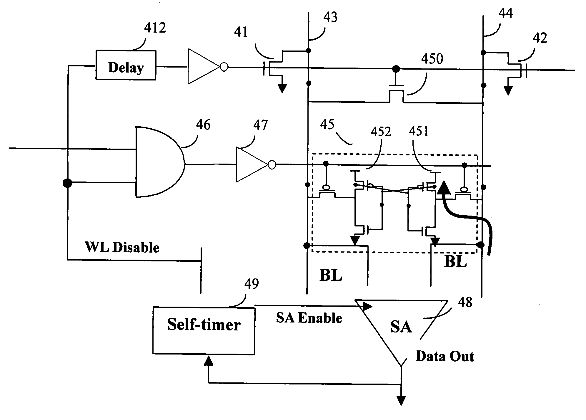
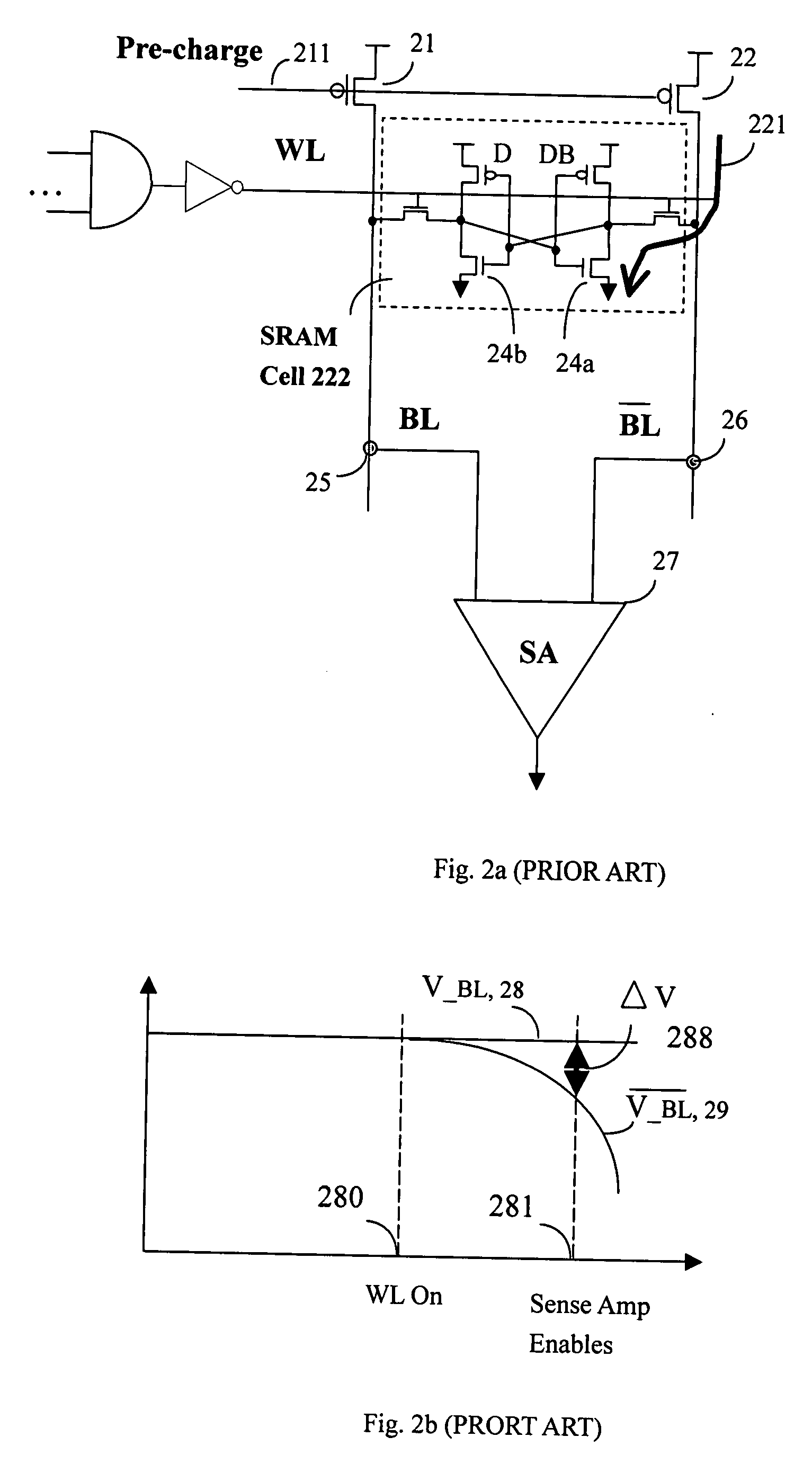
[0029]In addition to the parasitic diode leakage current, there are two main factors consuming power in semiconductor memory circuits. The first one is differentiating the voltage between bit line and bit line-bar which are input into the sense amplifier. The other is the leak current caused by the overlapping of pre-charging and word line signal. The operation of charging and discharging the bit line and bit line-bar results in power consumption. The equation below shows the power consumption calculation. CL is the capacitive loading, f is the switching frequency which is equivalent to charging and discharging frequency, delta V is the magnitude of the voltage swing. These three factors dominate the power consumption of the memory data sensing.

P=CL×ΔV2×f

[0030]External noise coupled into the sense amplifier causes the sense amplifier to inadvertently switch from one output voltage potential to another output voltage potential. That is, the noise coupled into the sense amplifier cau...


PUM


Abstract

The present invention provides a sensing scheme for semiconductor memory. N-type devices coupling between ground and a bit line and a bit line-bar of memory cells quickly discharge a bit line and a bit line-bar during non-accessing mode. During data accessing mode, one P-type device of an SRAM memory cell pulls up bit line or bit line-bar node slowly to minimize the inductive coupling noise and VDD, Ground bouncing, hence allows smaller amount of differential voltage input to the sense amplifier and results in lower power consumption. A self-timer counts the needed time and sends a signal to enable the current driven sense amplifier and to turn off the word line to avoid further pulling up the bit line or bit line-bar voltage and to reduce the power dissipation.

Description

BACKGROUND OF THE INVENTION[0001]1. Field of Invention[0002]This invention relates generally to a semiconductor memory sensing scheme. In particular, it relates to a pre-charging circuit for SRAM memory data accessing which connects to bit line and bit line-bar of semiconductor memory array which helps in reducing power consumption during accessing the memory cell.[0003]2. Description of Related Art[0004]A semiconductor memory is typically comprised of an array of memory cells which are aligned in rows and columns as shown in FIG. 1. A memory cell 14 is used to store data for future use. For efficiency, a memory array includes a large amount of memory cells 14. A WL 15 runs through top of hundreds or even thousands of memory cell gates which makes the WL 15 capacitance load quite large and needs a big driver 13 to turn on the WL 15.[0005]In an CMOS circuit, “Ground, or 0V” is mostly commonly used to represent a logic “0”, while a “Supply voltage, VDD” is mostly commonly used to repr...

Claims


Application Information

Patent Timeline
IPC IPC(8): G11C7/08G11C7/12
CPCG11C7/08G11C11/413G11C11/412G11C7/12
Inventor SUNG, CHIH-TA STAR
Owner TAIWAN IMAGINGTEK
Why Eureka
Try Eureka