Dead-time compensation method for electric drives

a technology of electric drives and dead-time compensation, which is applied in the direction of dc-ac conversion without reversal, process and machine control, instruments, etc., can solve the problems of additional voltage output deviation of inverter, switching between non-inverted and inverted carrier signals,

Inactive Publication Date: 2007-10-23
GM GLOBAL TECH OPERATIONS LLC
View PDF10 Cites 19 Cited by
  • Summary
  • Abstract
  • Description
  • Claims
  • Application Information

AI Technical Summary

Benefits of technology

[0023]Embodiments of the invention provide a method for compensating for dead-time in an inverter including a first switch and a second switch and a node disposed between the first switch and the second switch, the node including a current polarity. In one embodiment, the method comprises the steps of inserting a dead-time period prior to actuating ON the first switch and the second switch, pre-determining an amount of output in volt•seconds for the inverter, determining input signal including a pulse width for the inverter, wherein the output is based on the pulse width and the pulse width is based on a first carrier signal including a first pulse sequence, a second carrier signal including a second pulse sequence, wherein the first pulse sequence and the second pulse sequence are each one of a non-inverted pulse sequence and an inverted pulse sequence, and a polarity of current at the node, wherein the polarity is one of positive and negative, adding a first amount of pulse width to the input signal when the current polarity is positive, subtracting a second amount of pulse width from the input signal when the current polarity is negative, and determining if an additional amount of pulse width needs to be added to or subtracted from the input signal. In addition, embodiments of the invention include a computer-readable medium storing executable computer program instructions which, when executed by a processor, cause the processor to perform the method for compensating for dead-time in the inverter.

Problems solved by technology

However, switching between non-inverted and inverted carrier signals, even occasionally, may present another problem since the transition between pulse sequence types may require an additional period of dead-time per cycle, in addition to the already one dead-time period per cycle methods represented by timing diagrams 200 and 300.
Moreover, when the carrier signal transitions from a non-inverted to an inverted carrier signal or from an inverted to a non-inverted carrier signal, an additional dead-time period is needed to prevent shoot-through failures, which results in additional voltage output deviation for inverter 100.

Method used


Image

  • Dead-time compensation method for electric drives
  • Dead-time compensation method for electric drives
  • Dead-time compensation method for electric drives

Examples


Embodiment Construction

[0036]The following detailed description of the invention is merely exemplary in nature and is not intended to limit the invention or the application and uses of the invention. Furthermore, there is no intention to be bound by any theory presented in the preceding background of the invention or the following detailed description of the invention.

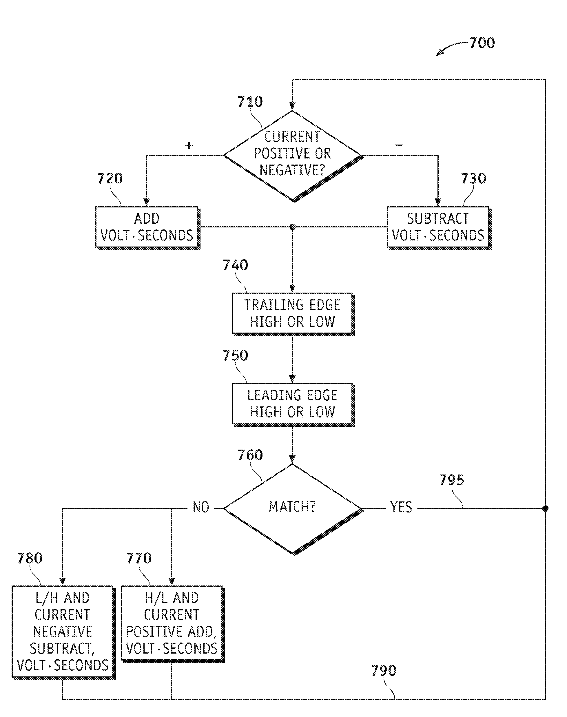
[0037]FIG. 7 is a flow diagram illustrating one embodiment of a method 700 for compensating for a deviation in output voltage in an inverter (e.g., inverter 100) when dead-time periods are utilized to prevent a shoot-through failure. In accordance with one embodiment, method 700 initiates by determining whether the current at node 130 is positive or negative when a current carrier signal arrives at inverter 100 (step 710).

[0038]When the current at node 130 is positive, in one embodiment, method 700 includes adding volt•seconds to the input signal of inverter 100 (step 720). When the current from node 130 is negative, in one embodiment, metho...


PUM


Abstract

Methods and apparatus are provided for compensating for a deviation in voltage output of a phase leg inverter when dead-time periods are inserted to prevent shoot-through failures. The method includes determining a pulse width for an input signal to the inverter such that the inverter voltage output is a desired amount. The pulse width is based on the non-inverted or inverted pulse sequences of two carrier signals and the polarity of current through the inverter. An amount of pulse width is added to the input signal when the current is positive, and an amount of pulse width is subtracted from the input signal when the current is negative. An additional amount of pulse width is added to or subtracted from the input signal depending on whether the carrier signal sequence changes from a non-inverted signal to an inverted signal or changes from an inverted signal to a non-inverted signal, respectively.

Description

TECHNICAL FIELD[0001]The present invention generally relates to semiconductor devices, and more particularly relates to a phase leg inverter.BACKGROUND OF THE INVENTION[0002]Inverters (e.g., a phase leg inverter) are utilized for a variety of electrical applications. FIG. 1, for example, is a diagram of a prior art phase leg inverter 100 having a voltage rail 108 coupled to a ground rail 118. Voltage rail 108 generally includes a switch 110 coupled in parallel with a diode 115 and, ground rail typically includes a switch 120 coupled in parallel with a diode 125, wherein diodes 115 and 125 are anti-parallel with respect to one another. Moreover, voltage rail 108 and ground rail 118 include a node 130 disposed between them such that positive current flows from ground through diode 125 (or through switch 120 when ON), and negative current flows to a voltage source through diode 115 (or through switch 110 when ON) when switches 110 and 120 are simultaneously OFF.[0003]In typical phase l...

Claims


Application Information

Patent Timeline
Patent Type & Authority Patents(United States)
IPC IPC(8): H02M1/12H02M7/44H02M7/68
CPCH02M7/53803H02M2001/385H02M1/385
Inventor WELCHKO, BRIAN AHITI, SILVASCHULZ, STEVEN E.
Owner GM GLOBAL TECH OPERATIONS LLC
Why Eureka
Try Eureka