Method for producing a cover, method for producing a packaged device

a packaging device and cover technology, applied in the field of packaging devices, can solve the problems of high price, affecting the mechanical properties of mechanically sensitive parts, and using ceramic packaging, etc., and achieve the effects of convenient processing, reduced price, and easy adhesion

Active Publication Date: 2007-10-30
CHEMTRON RES
View PDF12 Cites 208 Cited by
  • Summary
  • Abstract
  • Description
  • Claims
  • Application Information

AI Technical Summary

Benefits of technology

[0008]It is the object of the present invention to provide a cost-effective, but nevertheless safe concept for packaging sensitive devices.
[0011]As a material for the frame structure and the cap structure, a photostructurable material and, in particular, a relatively thick epoxy resin is used. This epoxy resin, that is spun onto the wafer in a liquid state, is stable and easily processable in the cured state, may further be easily adhered and, as compared to a silicon wafer or a quartz wafer, is available at a considerably lower price. If the epoxy resin for the cap structure is arranged on the support wafer by means of a sacrificial layer, it has the further advantage that the sacrificial layer may be detached selectively so that only the cap layer remains on the system wafer and particularly on the frame structure of the system wafer. The selective detachability has the further advantage that the support wafer is not affected by the detaching process of the sacrificial layer and thus may be reused so that a further cost reduction is possible.

Problems solved by technology

Typical packaging concepts, such as casting or molding in plastic or resin, are disadvantageous in that the mechanical properties of mechanically sensitive parts may be affected, or, like in the case of BAW or SAW filters, in that the material on the surface of the BAW resonators also has an influence on the characteristics of the filter.
Alternatively, ceramic packages also are employed, which are, however, expensive.

Method used


Image

  • Method for producing a cover, method for producing a packaged device
  • Method for producing a cover, method for producing a packaged device

Examples


Embodiment Construction

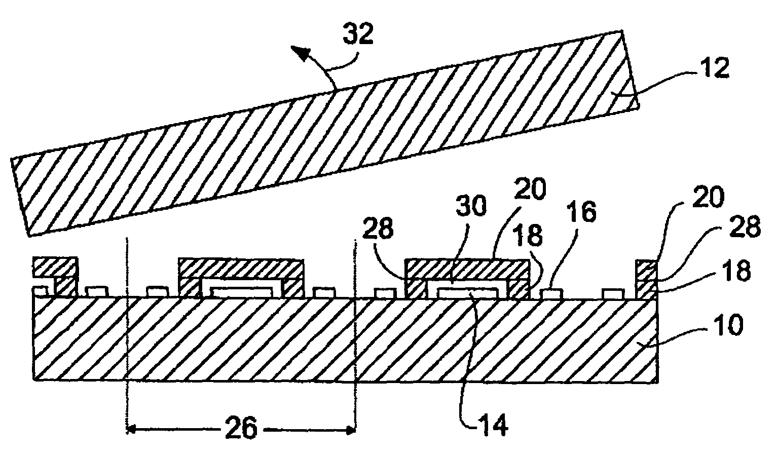
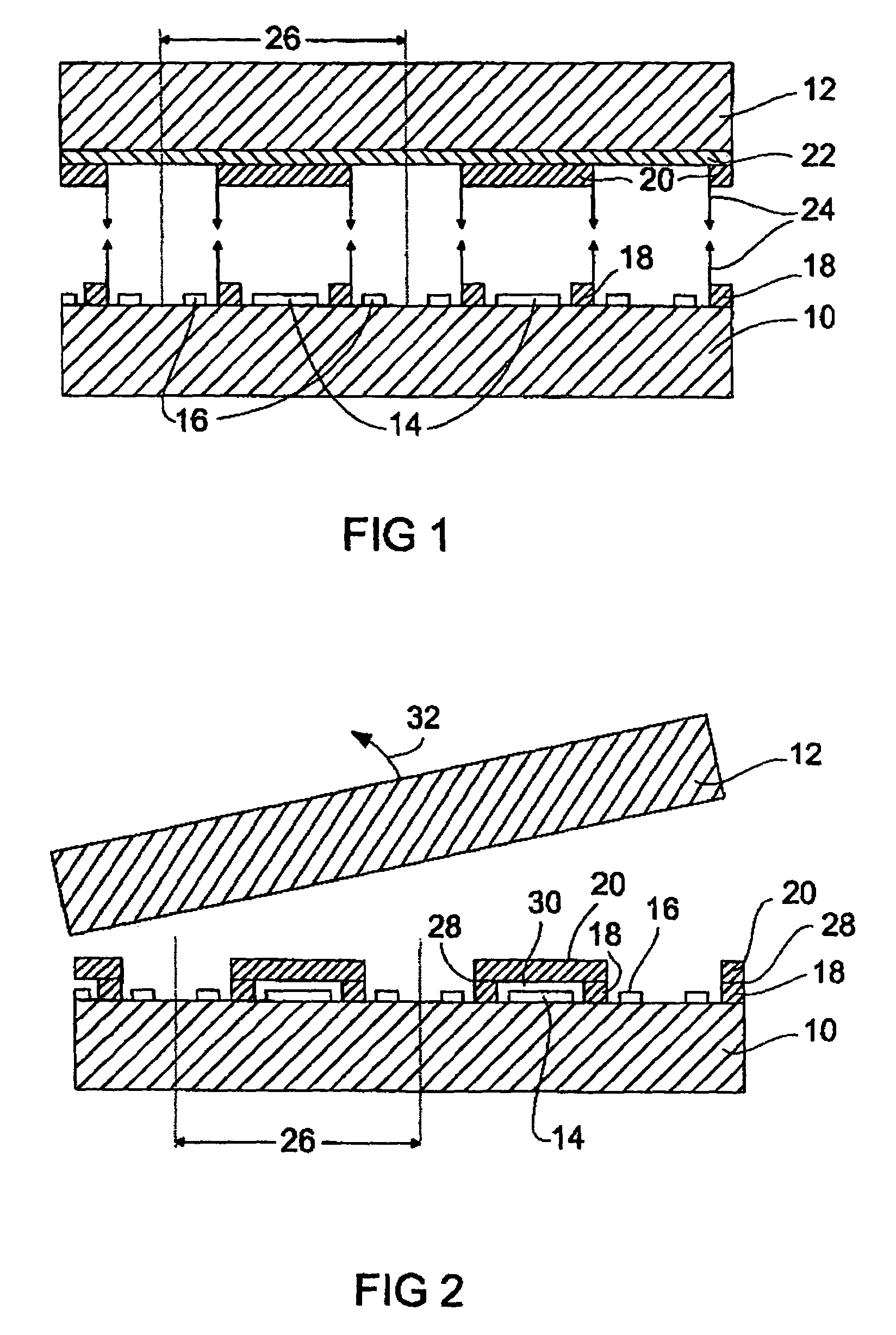
[0015]FIG. 1 depicts a system wafer 10 and a support wafer 12, wherein devices 14 that may be contacted via contact pads 16 are arranged on the system wafer 10. The devices 14 may either be applied to the system wafer 10 as discrete elements, for example by adhering, flip chip mounting, etc., or may be integrated in the system wafer 10. The devices are, for example, BAW or SAW filters, resonators, sensors, or actuators, or generally devices containing a region 14 that is to be protected, i.e. to be provided with a cover according to the invention. A frame structure 18 is arranged around the devices 14, that, depending on the application, either encloses the devices completely or, for example, encloses the devices only on two sides as viewed from above. The frame structure 18 may also be interrupted when it encloses the devices completely. It only has to be implemented in such a way that it may carry a cap structure 20. If the frame structure is interrupted, however, it does not prot...


PUM


Abstract

In a method for producing a cover for a region of a substrate, first a frame structure is produced in the region of the substrate, and then a cap structure is attached to the frame structure so that the region under the cap structure is covered. Thus, sensitive devices may be protected easily and at low cost from external influences and particularly from a casting material for casting the entire packaged device, which results when a diced chip is cast.

Description

CROSS-REFERENCE TO RELATED APPLICATION[0001]This application is a continuation of copending International Application No. PCT / EP03 / 00691, filed Jan. 23, 2003, which designated the United States and was not published in English.BACKGROUND OF THE INVENTION[0002]1. Field of the Invention[0003]The present invention relates to packaged devices and particularly to packaged devices containing mechanically sensitive components. A mechanically sensitive component or an active region, respectively, is, for example, an SAW or BAW filter or a micromechanical element.[0004]2. Description of the Related Art[0005]Micromechanical devices play an increasingly important role, particularly when considering rotation rate sensors, acceleration sensors, etc. Here, a mechanically active part such as a mass that is deflectable depending on acceleration, or a vibrator that may be put in stimulating vibration in a rotation rate sensor, or generally a sensor or actuator is packaged together with an integrated...

Claims


Application Information

Patent Timeline
Patent Type & Authority Patents(United States)
IPC IPC(8): H01L21/00H01L21/48H01L21/50B81B7/00H03H9/10
CPCH03H9/1071H03H9/105
Inventor AIGNER, ROBERTFRANOSCH, MARTINMECKES, ANDREASOPPERMANN, KLAUS-GUENTERSTRASSER, MARC
Owner CHEMTRON RES
Why Eureka
Try Eureka