Plasma display panel and method for manufacturing the same

a technology for plasma display panels and plasma, which is applied in the manufacture of electrode systems, electric discharge tubes/lamps, and electrodes, etc., can solve the problems of affecting the image quality of the panel, affecting the quality of the image, and affecting the quality of the panel. , to achieve the effect of improving the image quality of the plasma display panel

Inactive Publication Date: 2007-11-06
LG ELECTRONICS INC
View PDF9 Cites 4 Cited by
  • Summary
  • Abstract
  • Description
  • Claims
  • Application Information

AI Technical Summary

Benefits of technology

[0024]An object of the present invention is to provide a PDP and method for manufacturing the same wherein the quality of an image is improved by preventing an erroneous discharge.
[0027]According to a PDP and method for manufacturing the same of the present invention, since an erroneous discharge does not occur, the quality of an image of a plasma display panel is improved.

Problems solved by technology

However, since unwanted wall charges are formed on the barrier ribs of the PDP and the wall charges formed in a scan / sustain electrode 12Y are removed by these wall charges, erroneous discharge frequently occurs.
Thereby, there occurs a problem in that the quality of an image is degraded since an erroneous discharge occurs in the PDP, which affects the image quality of a panel.

Method used


Image

  • Plasma display panel and method for manufacturing the same
  • Plasma display panel and method for manufacturing the same
  • Plasma display panel and method for manufacturing the same

Examples


Embodiment Construction

[0039]Preferred embodiments of the present invention will be described in a more detailed manner with reference to the drawings.

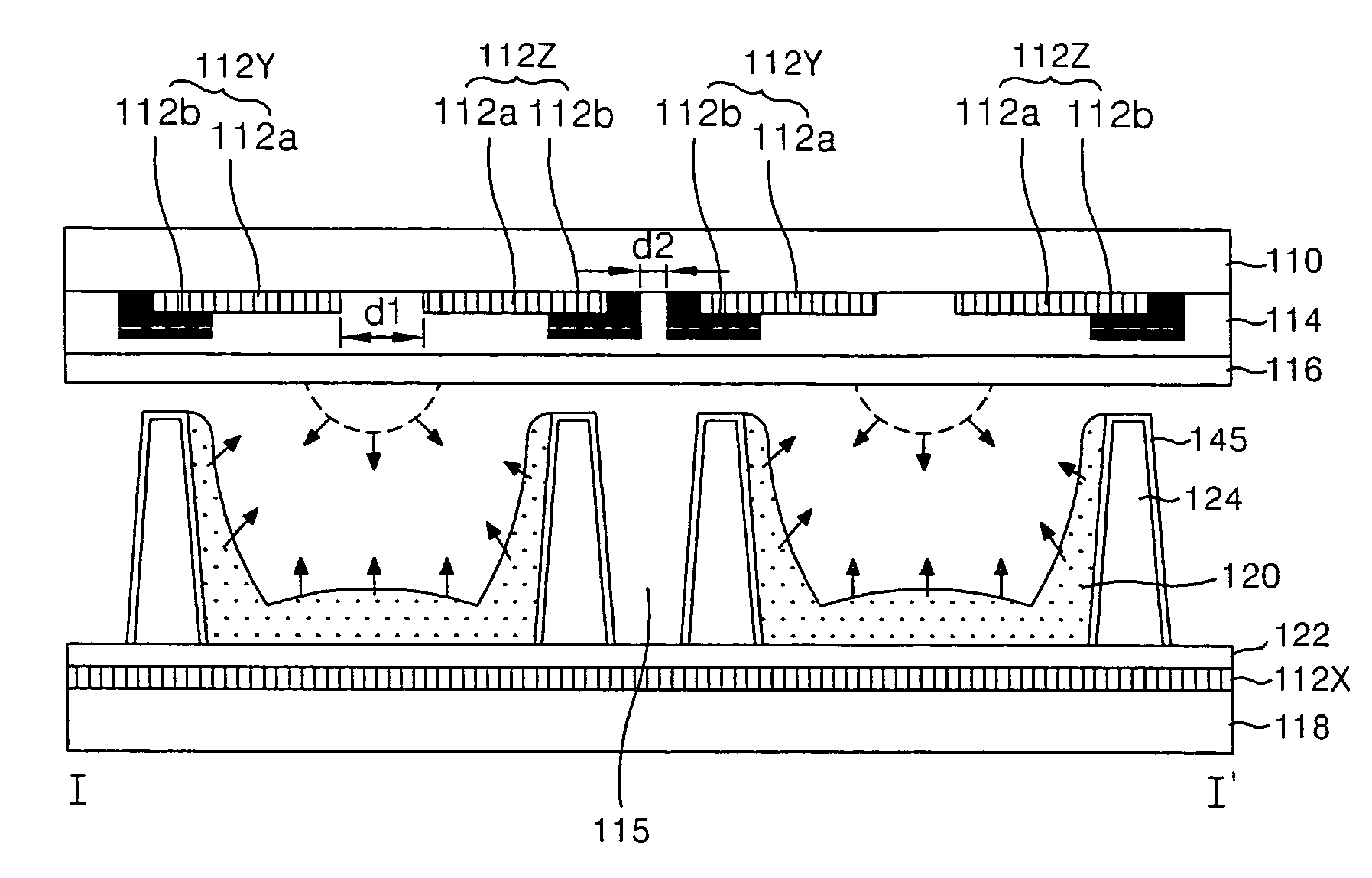
[0040]A plasma display panel may hereafter be described as having a plurality of discharge cells, including barrier ribs by which a discharge space is defined between an upper substrate and a lower substrate, and an oxide film of a low dielectric constant formed on each of the barrier ribs.

[0041]The oxide film of the plasma display panel may include at least one of silicon oxide and magnesium oxide.

[0042]The plasma display panel may further include a first electrode formed on the underside of the upper substrate and a second electrode formed on the underside of the upper substrate in such a manner as to extend over the first electrode.

[0043]A first barrier rib may be arranged in parallel with the first and second electrodes and have an auxiliary discharge space. A second barrier rib may be arranged to intersect the first barrier rib.

[0044]A method for manuf...


PUM


Abstract

The present invention discloses a plasma display panel and method for manufacturing the same wherein the quality of an image can be improved by preventing an erroneous discharge. A plasma display panel having a number of discharge cells according to an embodiment of the present invention includes barrier ribs by which a discharge space is defined between an upper substrate and a lower substrate; and an oxide film of a low dielectric constant formed on each of the barrier ribs. A method for manufacturing a plasma display panel according to an embodiment of the present invention includes the steps of: forming barrier ribs on a lower substrate so that a discharge space is defined by the barrier ribs between an upper substrate and a lower substrate; and forming an oxide film of a low dielectric constant on each of the barrier ribs. According to a PDP and method for manufacturing the same of the present invention, since an erroneous discharge does not occur, the quality of an image of a plasma display panel is improved.

Description

[0001]This Nonprovisional application claims priority under 35 U.S.C. § 119(a) on Patent Application No. 10-2003-0048732 filed in Korea on Jul. 16, 2003, the entire contents of which are hereby incorporated by reference.BACKGROUND OF THE INVENTION[0002]1. Field of the Invention[0003]The present invention relates to a plasma display panel and method for manufacturing the same, and more particularly, to a plasma display panel and method for manufacturing the same wherein the quality of an image can be improved by preventing an erroneous discharge.[0004]2. Description of the Background Art[0005]Various flat panel display devices have recently been developed which can reduce their heavy weight and large volume as shortcomings of the cathode ray tube. These flat panel display devices include a liquid crystal display (LCD), a field emission display (FED), a plasma display panel (hereinafter, referred to as “PDP”), an electro-luminescence (EL) display device and so on.[0006]Among them, the...

Claims


Application Information

Patent Timeline
Patent Type & Authority Patents(United States)
IPC IPC(8): H01J17/49H01J9/02H01J9/00H01J9/24H01J11/12H01J11/22H01J11/24H01J11/26H01J11/34H01J11/36H01J17/02
CPCH01J9/242H01J11/12H01J11/36H01J2211/366H01J2211/323H01J11/40
Inventor RHEE, BYUNG JOON
Owner LG ELECTRONICS INC
Why Eureka
Try Eureka