Method to locate logic errors and defects in digital circuits

a logic error and digital circuit technology, applied in the field of digital circuits, can solve problems such as error detection and error generation

Active Publication Date: 2007-11-13
DAFCA
View PDF3 Cites 209 Cited by
  • Summary
  • Abstract
  • Description
  • Claims
  • Application Information

AI Technical Summary

Problems solved by technology

Illustratively, an error is detected in the course of assertion checking with an assertion-checking circuit provisioned within a wrapper of the IC.
Typically, the error path will lead to a small subcircuit where the error is generated.

Method used


Image

  • Method to locate logic errors and defects in digital circuits
  • Method to locate logic errors and defects in digital circuits
  • Method to locate logic errors and defects in digital circuits

Examples


Embodiment Construction

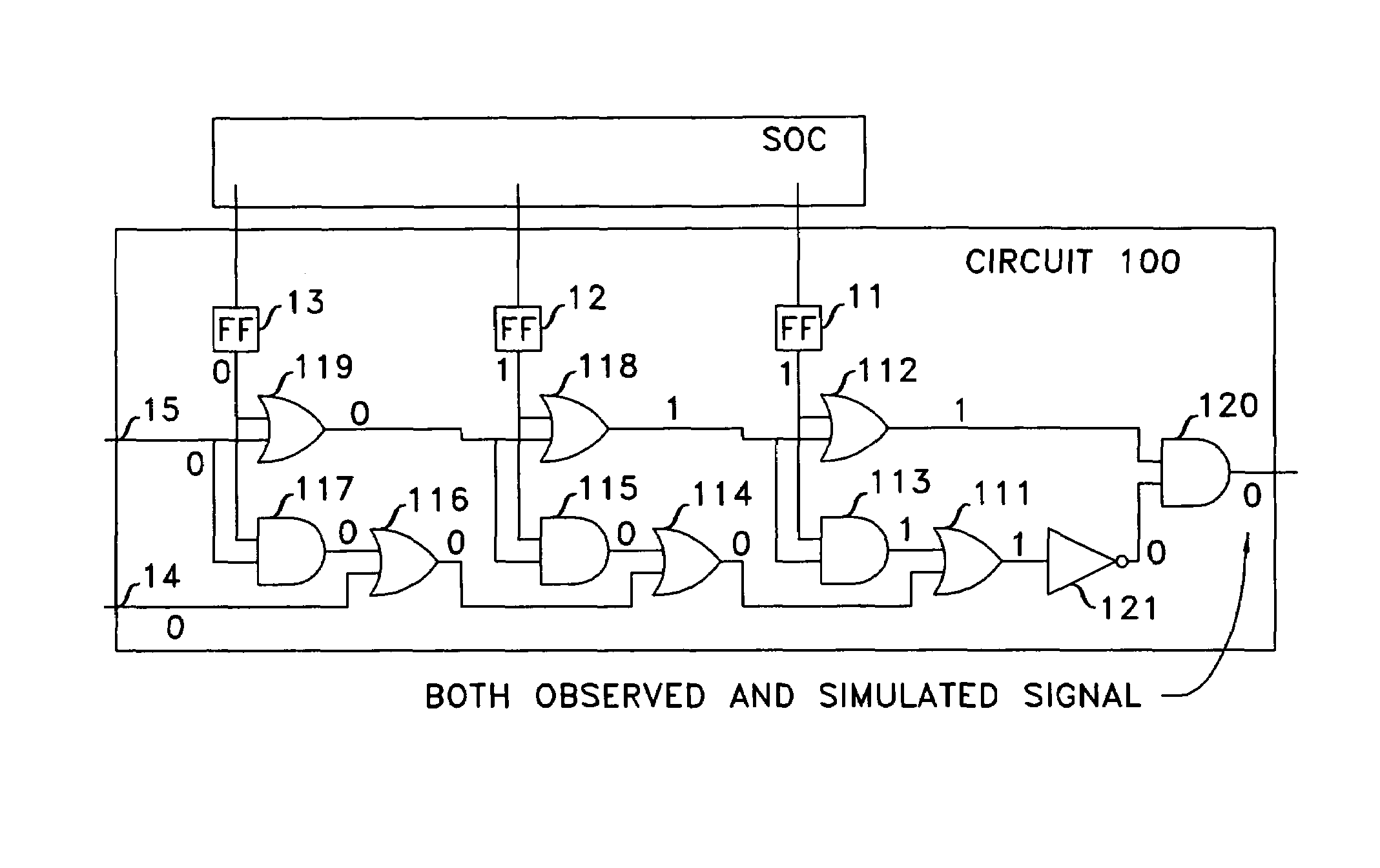
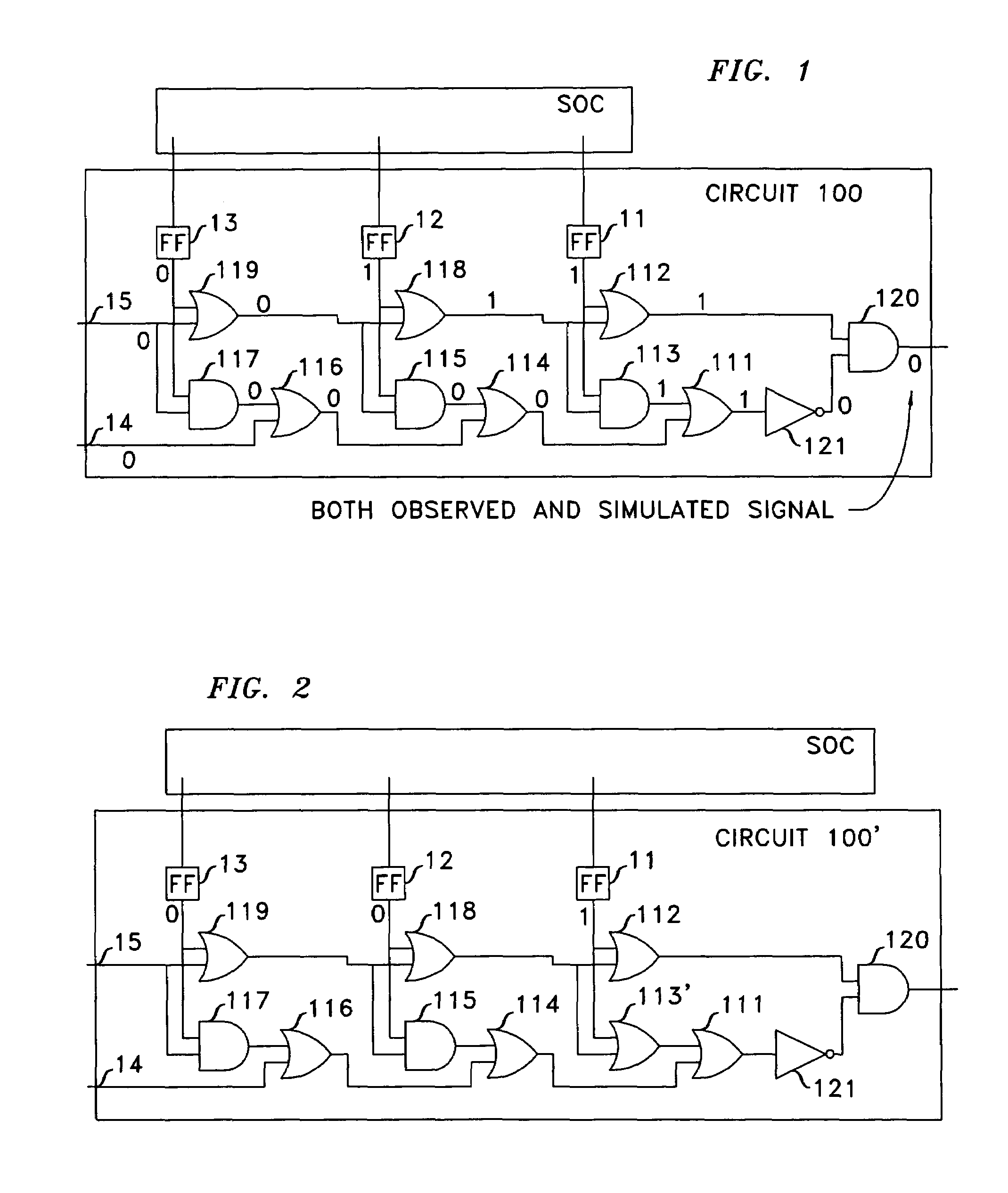
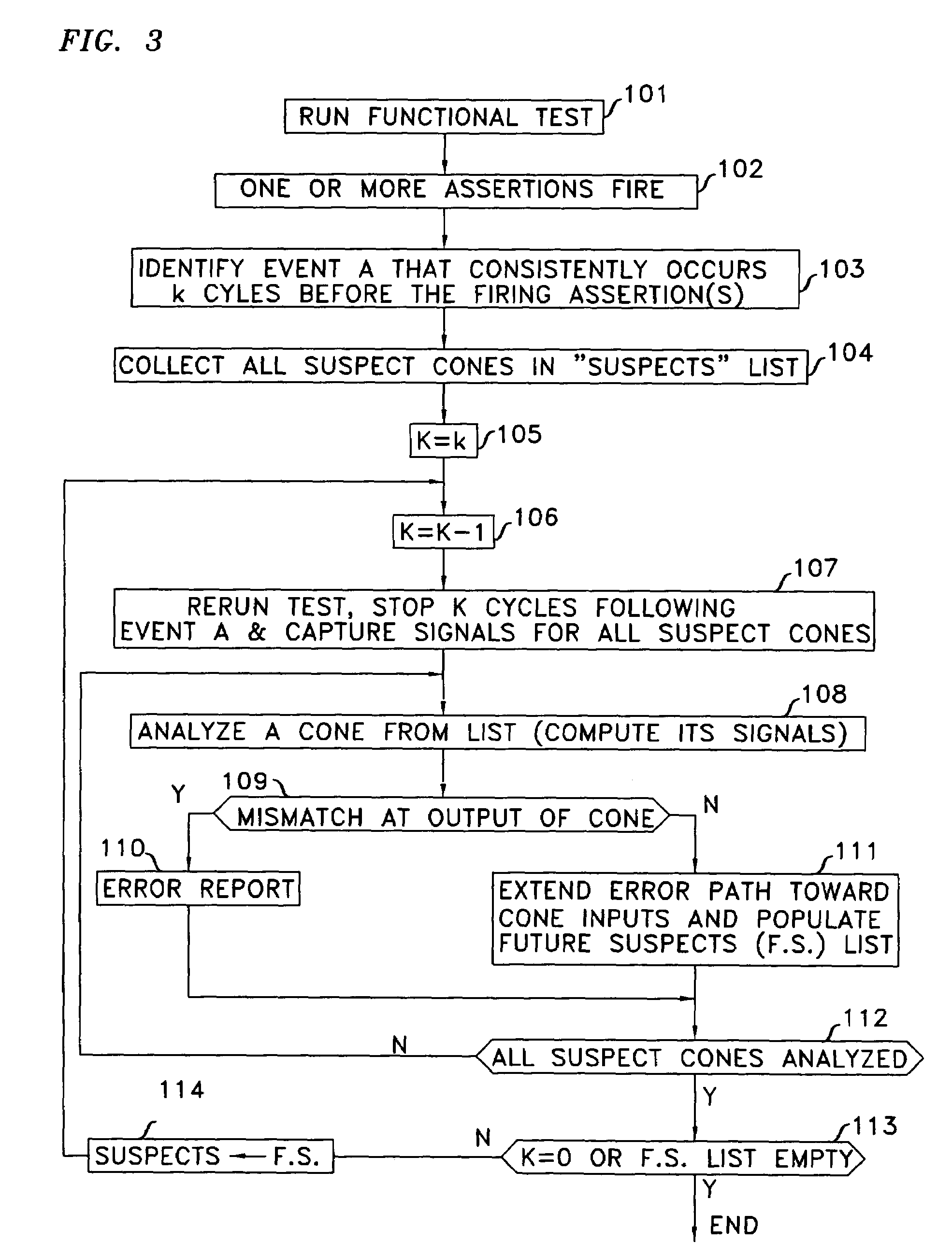
[0016]The principles disclosed herein are applicable to integrated circuits where the values of at least some internal signals can be observed. Since in most ICs all flip-flops have a mode of operation in which they are connected to form shift registers (scan chains), their values can be read by a scan-out operation when the normal operation has been stopped, and therefore, the principles disclosed herein have wide applicability and are of great advantage to the field of IC design, manufacturing, and testing.

[0017]At the outset, it is useful to define the notions of a “fanin cone” and a “suspect cone” as used herein. In its simplest form, a “fanin cone” is a single-output circuit that corresponds to that portion of possibly a larger combinatorial circuit (for example, within an IC) that potentially affects the value of that single output. The input signals of a fanin cone are either primary inputs of the IC (whether it is an SoC or not), or output signals of memory elements within t...


PUM


Abstract

When, in the course of an integrated circuit's functional test an assertion fires at clock k, the operational clock is stopped, the sequence is reapplied to capture inputs to the assertion circuit that fired, signals within the assertion circuit are computed, and the error is backtraced. Once one or more inputs of the assertion circuit are identified as potentially the source of the error, the process of backtracing is performed for each such input. When the input that is potentially the source of the error emanates from a memory circuit, the fanin cone of the memory circuit is identified and the process of backtracing through the last-identified fanin cone is undertaken for clock k−1. This is repeated iteratively until either a module of the integrated circuit is found to be the source of the error, or the error is extended to inputs of the SoC.

Description

RELATED APPLICATIONS[0001]This invention is related to U.S. patent application Ser. No. 10 / 425,101, filed Apr. 28, 2003, to U.S. patent application Ser. No. 10 / 929,709 filed Aug. 30, 2004, to U.S. patent application Ser. No. 10 / 956,854, filed Oct. 1, 2004, to U.S. patent application Ser. No. 11 / 051,774 filed Feb. 4, 2005, and to U.S. patent application Ser. No. 11 / 136,993 filed May 25, 2005, which are hereby incorporated by reference.FIELD OF THE INVENTION[0002]This invention relates to digital circuits and, more particularly, to functional testing and debugging of integrated circuits (ICs).BACKGROUND OF THE INVENTION[0003]After an integrated circuit is manufactured, it is typically tested both to check that manufacturing defects are not present in the silicon (manufacturing testing), and to verify that it correctly performs its specified function (functional testing). While manufacturing test is done with a tester, functional testing is typically done “in-system,” where the target ...

Claims


Application Information

Patent Timeline
Patent Type & Authority Patents(United States)
IPC IPC(8): G01R31/28
CPCG01R31/318544
Inventor ABRAMOVICI, MIRON
Owner DAFCA
Why Eureka
Try Eureka