Method and apparatus for verifying semiconductor integrated circuits

a technology of integrated circuits and verification methods, applied in software simulation/interpretation/emulation, instruments, program control, etc., can solve the problems of short affecting the accuracy of timing checks, etc., to achieve the effect of short pulse width and lengthening the design time of semiconductor integrated circuits

Inactive Publication Date: 2007-11-20
FUJITSU MICROELECTRONICS LTD
View PDF11 Cites 19 Cited by
  • Summary
  • Abstract
  • Description
  • Claims
  • Application Information

AI Technical Summary

Benefits of technology

[0011]However, when the number of buffer circuits 111 increases as shown in FIG. 2(a), the amount of delay variations accumulated from the input terminal of the clock signal CK to the input terminal of the flip flop circuit 112 is large. In this case, the signal may have an extremely short pulse width, with its rising edge being close to its falling edge. If this happens, the pulse width of signals provided to input terminals of many circuits is determined as having an error. This requires such measures as delaying signal timings to be taken, and as a result, lengthens the design time for semiconductor integrated circuits.
[0014]The present invention provides a method and apparatus that enable accurate verifying while considering on-chip variations.

Problems solved by technology

This requires such measures as delaying signal timings to be taken, and as a result, lengthens the design time for semiconductor integrated circuits.
However, only one of a rise delay and a fall delay is set to consider delay variations in the timing verification of the prior art.
Thus, the prior art verification fails to provide a correct verification result.
Thus, the timing check may be executed under an extremely strict condition, or under an impractical condition.
However, when the timing check considering delay variations of the clock signal CK is executed, the hold time HT may fail to satisfy its standards (the hold time HT may be shorter than its standard time).
If this happens, the operation of the flip flop is not ensured.
This requires such measures as delaying signal timings to be taken, and as a result, lengthens the design time of semiconductor integrated circuits.

Method used


Image

  • Method and apparatus for verifying semiconductor integrated circuits
  • Method and apparatus for verifying semiconductor integrated circuits
  • Method and apparatus for verifying semiconductor integrated circuits

Examples


Embodiment Construction

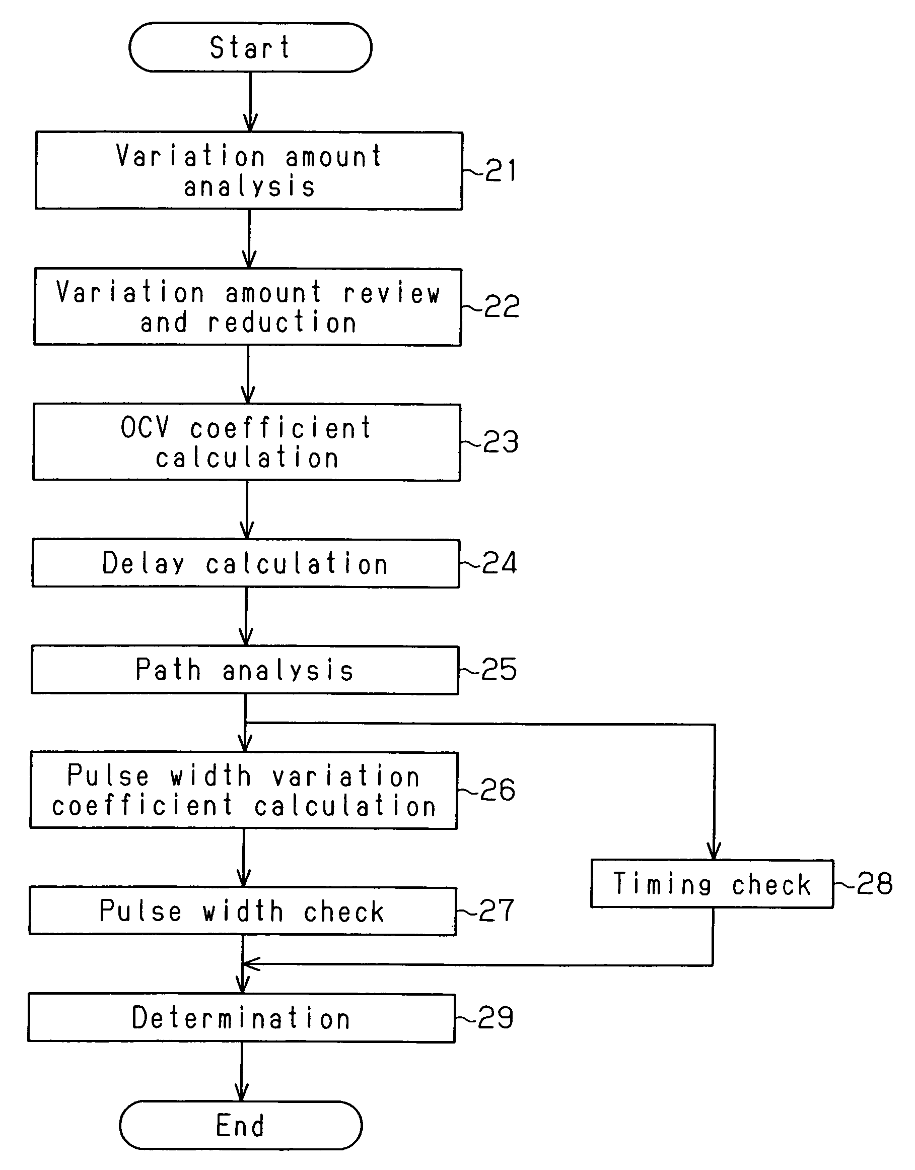
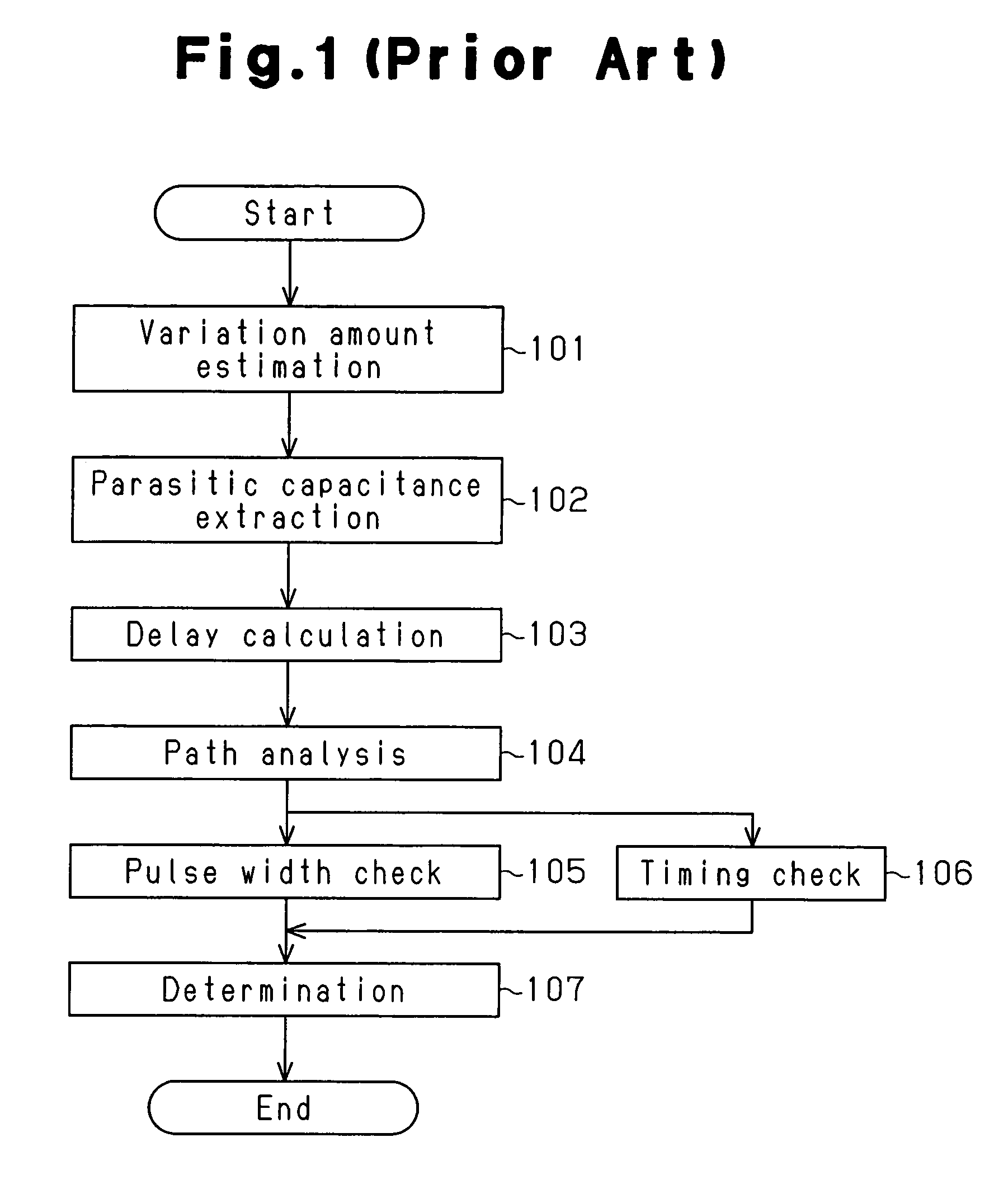
[0039]A timing verification apparatus 11 according to a preferred embodiment of the present invention will now be discussed, with reference to FIGS. 4 to 18.

[0040]FIG. 5 is a schematic block diagram of the timing verification apparatus 11.

[0041]The timing verification apparatus 11 is a computer aided design (CAD) apparatus, and includes a central processing unit (CPU) 12, a memory 13, a storage device 14, a display device 15, an input device. 16, and a drive device 17, which are connected to one another via a bus 18. The CPU 12 functions as a calculation means, a comparison means, a determination means, and a verification means.

[0042]The CPU 12 executes a program using the memory 13 to execute a timing verification process. The memory 13 stores programs and data necessary for achieving a timing verification function. The memory 13 includes a cache memory, a system memory, and a display memory (not shown).

[0043]The display device 15 is used to display a layout screen, a parameter inp...


PUM


Abstract

A timing verification apparatus calculates a pulse width variation coefficient based on a pulse width of an input clock signal, a delay value of the clock signal, and an operation frequency. The apparatus then calculates the pulse width for a delayed clock signal provided to a clock input terminal of a flip flop (FF) using the pulse width variation coefficient. Further, the apparatus compares the calculated pulse width with a standard value. The timing verification apparatus calculates the pulse width of the delayed clock signal provided to the clock input terminal of the FF using the pulse width of the clock signal, and a rise delay and a fall delay of the path. The apparatus considers on-chip variations and accurately executes timing verification for signals.

Description

CROSS-REFERENCE TO RELATED APPLICATIONS[0001]This application is based upon and claims the benefit of priority from the prior Japanese Patent Application No. 2004-340797, filed on Nov. 25, 2004, the entire contents of which are incorporated herein by reference.BACKGROUND OF THE INVENTION[0002]The present invention relates to a method and apparatus for verifying semiconductor integrated circuits.[0003]The development of semiconductor integrated circuits includes the process of calculating delays in a logic circuit and verifying operation timings and delays in the logic circuit to check and ensure proper operation of the logic circuit. In recent years, semiconductor integrated circuits have a higher level of integration and operate at higher speeds and lower operation voltages. In such semiconductor integrated circuits, variations in power supply voltage drops within chips greatly affect delays and fluctuations in circuit operations. Thus, static timing analysis (STA) must be executed...

Claims


Application Information

Patent Timeline
Patent Type & Authority Patents(United States)
IPC IPC(8): G06F17/50
CPCG01R29/023G01R31/31725G01R31/3016
Inventor HOSONO, TOSHIKATSU
Owner FUJITSU MICROELECTRONICS LTD
Why Eureka
Try Eureka