Multi-row lead frame

a lead frame and multi-row technology, applied in the field of lead frame, can solve the problems of difficult to shape the tail end of the bond wire, the tail kink is sometimes too low, and the loop profile of the bond wire with the tail kink is often inconsisten

Inactive Publication Date: 2007-11-27
NORTH STAR INNOVATIONS
View PDF15 Cites 19 Cited by
  • Summary
  • Abstract
  • Description
  • Claims
  • Application Information

AI Technical Summary

Benefits of technology

[0025]As is evident from the foregoing discussion, the present invention provides a lead frame and a method of packaging a semiconductor device using the lead frame, which has benefits over existing products and processes. For example, by forming a step on the first (internal) row of terminals, the present invention ensures that tail kinks are consistently formed at a predetermined height in the bonding wires, thereby preventing wire damage during the packaging process. Additionally, the tail kinks can be formed using a conventional wire bonding process. Further, as the step functions as a support platform, wire sweep during a subsequent encapsulation process is prevented.

Problems solved by technology

However, because the bond wire is less rigid further away from the first wire bond, it is difficult to shape the tail end of the bond wire.
Hence, the loop profiles of bond wires with tail kinks are often inconsistent.
The tail kink is sometimes formed too low and the corresponding wire loop is susceptible to damage during subsequent packaging steps.

Method used


Image

  • Multi-row lead frame
  • Multi-row lead frame
  • Multi-row lead frame

Examples


Embodiment Construction

[0010]The detailed description set forth below in connection with the appended drawings is intended as a description of the presently preferred embodiments of the invention, and is not intended to represent the only form in which the present invention may be practiced. It is to be understood that the same or equivalent functions may be accomplished by different embodiments that are intended to be encompassed within the spirit and scope of the invention.

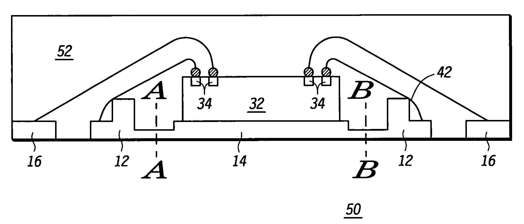
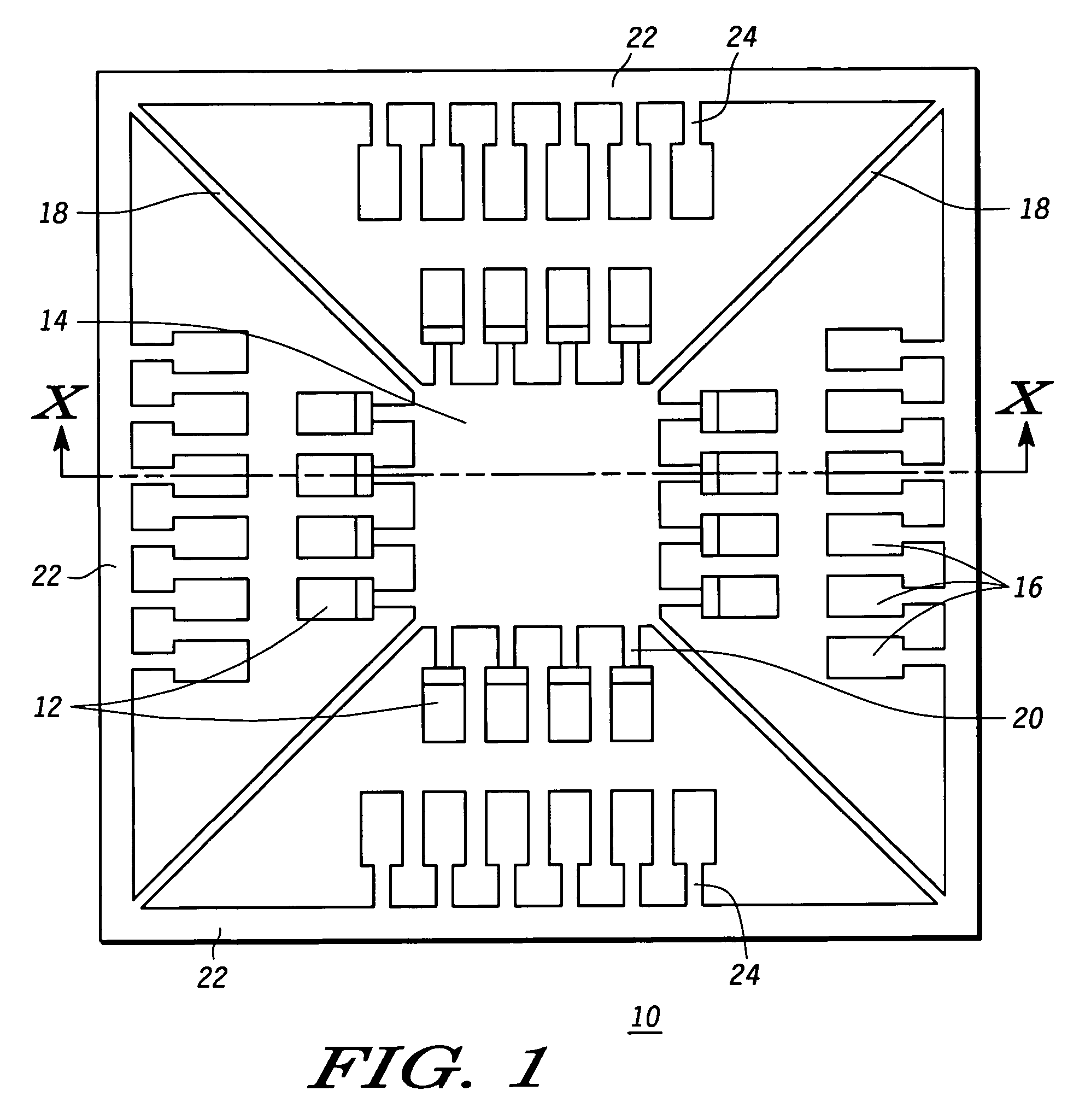
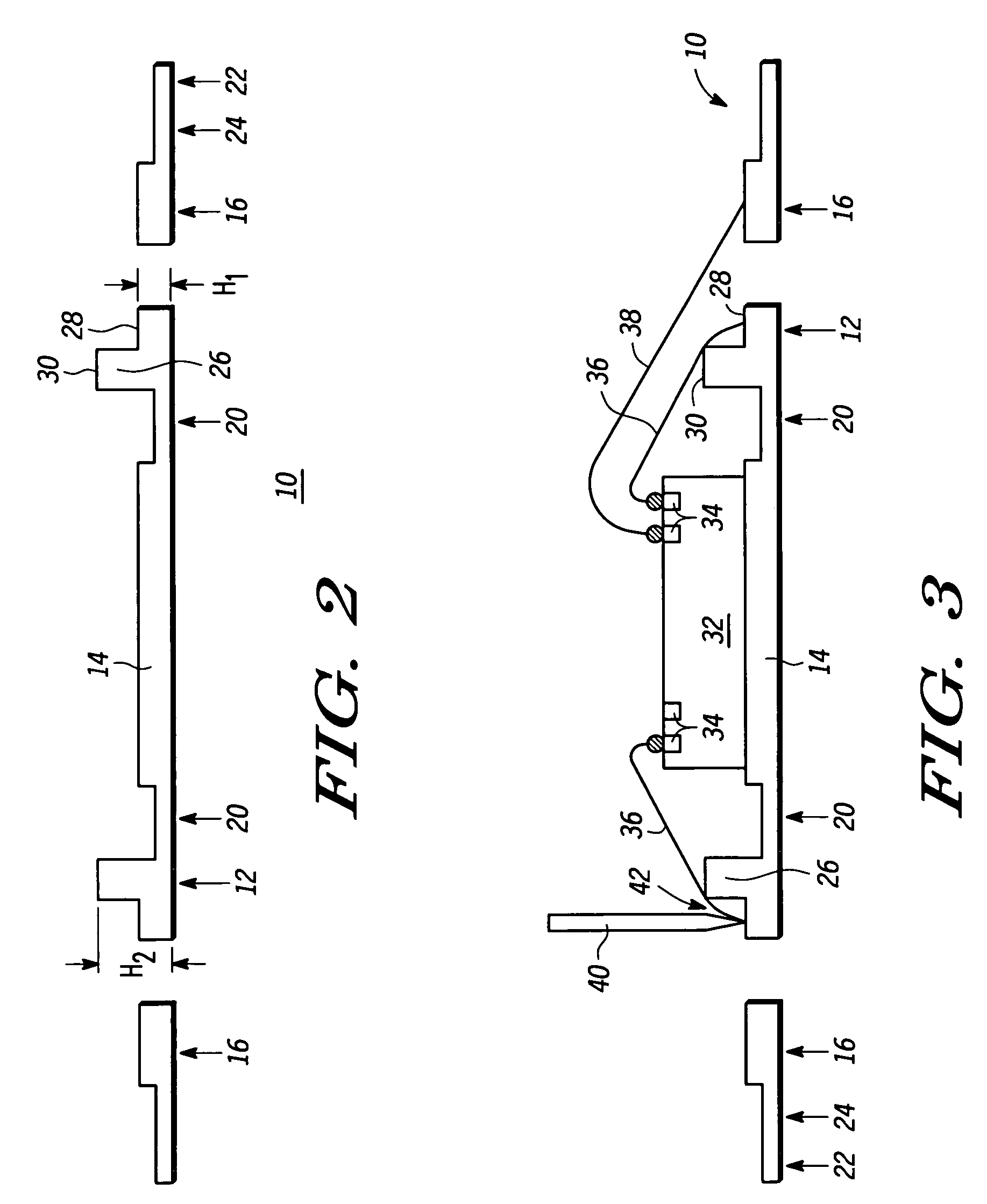
[0011]Certain features in the drawings have been enlarged for ease of illustration and the drawings and the elements thereof are not necessarily in proper proportion. Further, the invention is shown embodied in a quad flat no-lead (QFN) type package. However, those of ordinary skill in the art will readily understand the details of the invention and that the invention is applicable to other package types. In the drawings, like numerals are used to indicate like elements throughout.

[0012]In order to form a wire bonded semiconductor pac...


PUM


Abstract

A lead frame (10) for a semiconductor device includes a first row of terminals (12) surrounding a die receiving area (14) and a second row of terminals (16) spaced from and surrounding the first row of terminals (12). The first and second rows of terminals (12, 16) have a first height (H1). The terminals (12) of the first row include a step (26) that has a greater height (H2). Bond wires (36) connecting die pads (34) to the first row terminals (12) extend over the second height H2 part of the terminal (12) and are attached to the first height H1 part of the terminal (12). The step (26) insures that the bond wires (36) attached to the stepped terminals (12) have a high wire kink profile so that they are less susceptible to damage in later process steps.

Description

BACKGROUND OF THE INVENTION[0001]The present invention relates to semiconductor packaging in general and more specifically to a lead frame and a method of packaging a semiconductor device using such a lead frame.[0002]Wire bonding is widely used in semiconductor packaging to provide electrical connection between an integrated circuit (IC) die and a lead frame. In wire bonding applications, wire loops are formed between the die pads of an IC die and the lead fingers of a lead frame. Typically, first wire bonds are formed on respective ones of the die pads, and second wire bonds are formed on the corresponding terminals. Wire loops with a steep angle of approach to the second wire bond are required in certain applications, for example, to prevent damage during a singulating operation to separate the lead fingers from the die receiving area of the lead frame. Such loop profiles are created by forming a high tail kink in the bond wire, that is, a bend in the tail end of the bond wire at...

Claims


Application Information

Patent Timeline
Patent Type & Authority Patents(United States)
IPC IPC(8): H01L23/495H01L21/00H01L21/66
CPCH01L23/3107H01L23/49541H01L23/49548H01L24/48H01L2924/10253H01L2924/14H01L2924/01082H01L2924/01079H01L2924/01033H01L2924/01029H01L2924/01014H01L2924/01013H01L2924/01005H01L2924/01002H01L2224/78301H01L2224/48699H01L2224/48599H01L2224/48465H01L2224/48257H01L2224/48247H01L2224/48237H01L2224/48227H01L2224/48091H01L2224/45147H01L24/45H01L2224/45124H01L2224/45144H01L2924/00014H01L2924/00H01L2924/181H01L2224/49433H01L2924/00012H01L2224/85399H01L2224/05599
Inventor WONG, FEI YINGHO, WAI KEUNGWONG, HO WANG
Owner NORTH STAR INNOVATIONS
Why Eureka
Try Eureka