Power network reconfiguration using MEM switches

a technology of power network and switch, which is applied in the direction of process and machine control, semiconductor/solid-state device details, instruments, etc., can solve the problems of power supply distribution network beginning to face a tremendous challenge, slew rate, duty cycle, jitter, timing, etc., to be out of control, and no longer guarantee a predetermined voltage level at all corners of the chip

Inactive Publication Date: 2007-12-04
GLOBALFOUNDRIES INC
View PDF10 Cites 26 Cited by
  • Summary
  • Abstract
  • Description
  • Claims
  • Application Information

AI Technical Summary

Problems solved by technology

One conventional power mesh method (described in U.S. Pat. No. 6,480,989 incorporated herein by reference) to form a power supply distribution network begins to face a tremendous challenge.
It can no longer guarantee a predetermined voltage level at all corners of the chip.
In other words, the inevitable I*R voltage drop on the supply is known to cause problems, such as slew rate, duty cycle, jitter, timing, etc. to be out of control.
This impact has caused both high-speed analog and digital circuits to miss their performance targets and fail the specification.
One possible solution is to use low Vt devices to gain back some over-drivability; however, this is achieved at a cost of high power consumption which is undesirable.
One possible reason that this concept has not been implemented on the chip is lack of an efficient switch means which can easily be integrated with an IC chip to do the job.
There are many disadvantages of using semiconductor devices, either MOS or bipolar, for power switching.
So far, none of them has mentioned to use MEMS for designing a robust on-chip power distribution network.

Method used


Image

  • Power network reconfiguration using MEM switches
  • Power network reconfiguration using MEM switches
  • Power network reconfiguration using MEM switches

Examples


first embodiment

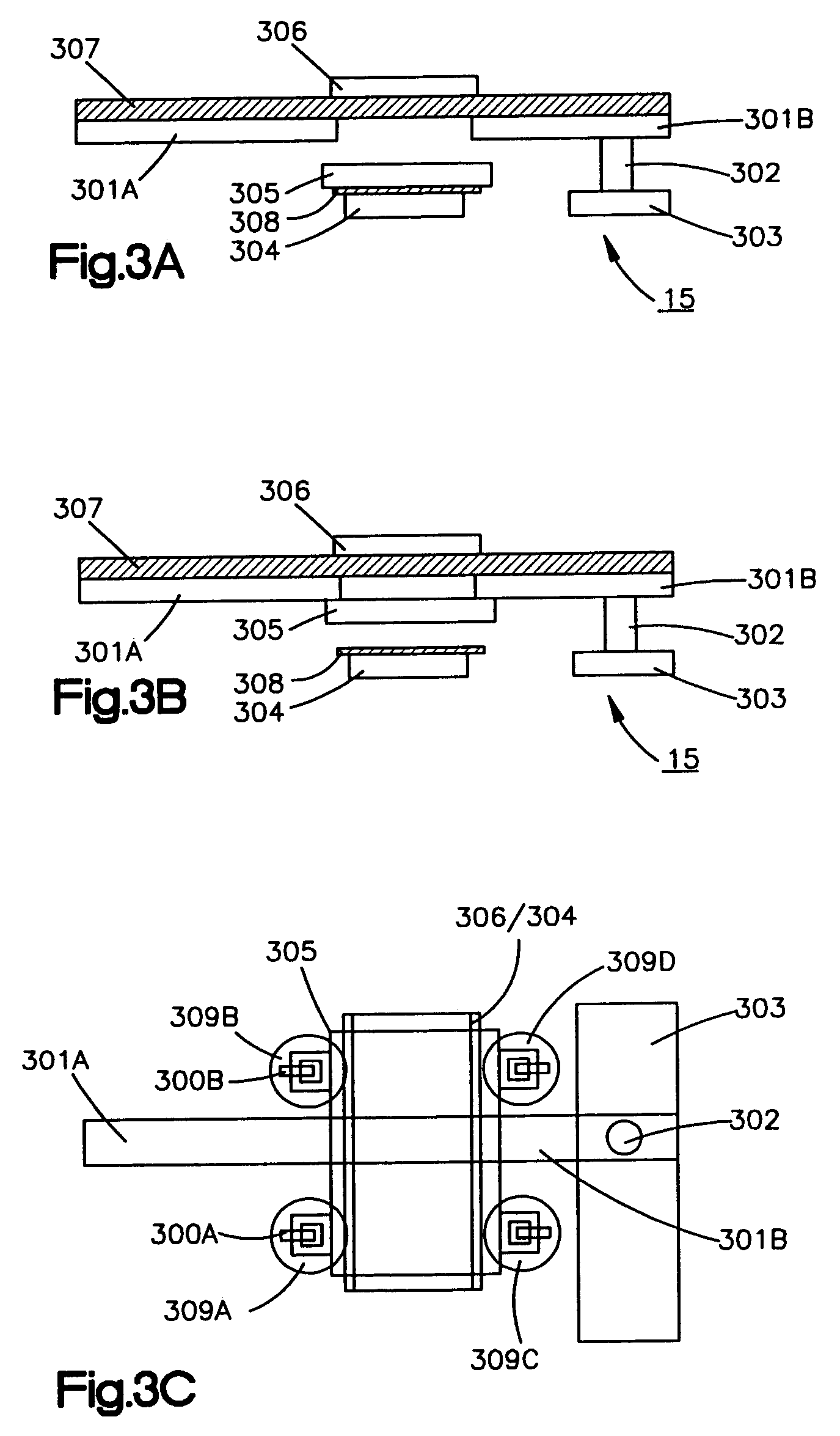
[0031]A first embodiment is a power steering switch device comprising at least one MEM switch component, so that during an early test mode, when one power supply is not available, the circuits and devices attached to that power supply can still be tested by borrowing power from another available power supply source. After testing and packaging, the MEM switch is turned off to completely isolate two power supply sources. In the past, MOS switches called “T-switches” were used to achieve this purpose. But, due to limited on-current capability, a large-size MOS switch is usually needed. There are many problems encountered with the T-switch which will be described in more detail infra. Two examples of T-switches are shown in FIGS. 4A and 4B.

[0032]In the past, a conventional CMOS T-switch device of the type shown in FIGS. 4A and 4B might be used so that network 502 can borrow power supply from Vdd. In this case, a control device 503 is needed to provide a control signal on line 506 to th...

second embodiment

[0034]The second embodiment is the use of a MEM switch to switch off unwanted or deactivated macros to thus isolate supply noise and cross-contamination between macros. At least one MEM switch can be used to switch “off” the power supply to each macro, so the leakage current, or Iddq of that macro can be measured. This technique can be used to detect and isolate faults caused by shorting.

third embodiment

[0035]The third embodiment is to use a MEM switch to perform pin reconfiguration. This feature is very powerful and useful especially when chip I / O numbers keep increasing. When a limited chip area cannot meet the I / O demand, many test functions or different operating modes must be abandoned. With reconfigurable pin scheme using at least one MEM switch, one can accommodate more testing features. After testing, the pins can be switched to power supply or other control or program pins to improve chip versatility.

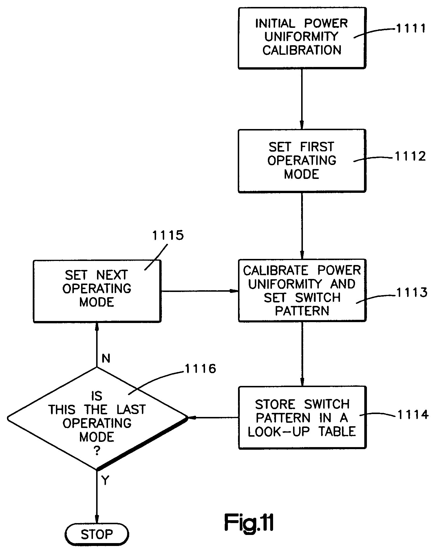
[0036]Another feature of this invention provides a robust and more dynamic power distribution network using MEM switches. This includes four embodiments: (1) a power distribution network using at least one MEM switch array with power sensing device, so that power can be distributed more uniformly to all corners of the chip. When a local sensing circuit detects low supply limit, the switch is automatically turned on and maintained on; (2) a power switching device comprising a h...


PUM


Abstract

A structure and method for power distribution to a network for an integrated circuit chip complex are provided. The chip complex has at least two sectors, each having at least one power providing connection with at least one of said connections beings individually addressable by, and isolatable from, a given power source. At least one MEMS is positioned to selectively connect and disconnect said at least one connection to and from said given power source.

Description

FIELD OF THE INVENTION[0001]This invention relates generally to reconfiguration of power networks of integrated circuit (IC) chip complexes using MEMS (microelectricalmechanical switch) to selectively switch power to selected portions of the chip complex.BACKGROUND OF THE INVENTION[0002]A robust power distribution network both for chips and packages is one of the critical tasks in integrated circuit (IC) design. As Moore's law continues to hold sway, more and more devices and circuits can be packed on a single chip. In the meantime, the silicon chip size also grows to accommodate the capability of multi-system integration. Furthermore, the required supply voltage is progressively reduced from one generation to another in order to save power. One conventional power mesh method (described in U.S. Pat. No. 6,480,989 incorporated herein by reference) to form a power supply distribution network begins to face a tremendous challenge. It can no longer guarantee a predetermined voltage leve...

Claims


Application Information

Patent Timeline
Patent Type & Authority Patents(United States)
IPC IPC(8): G06F1/00G06F1/32H02M3/335
CPCH01L23/50H01H59/0009H01L2924/3011H01L2924/0002H01L2924/00
Inventor CRANFORD, JR., HAYDEN C.HSU, LOUIS LU-CHENMASON, JAMES S.
Owner GLOBALFOUNDRIES INC
Why Eureka
Try Eureka