Image sensors with optical trench

a technology of image sensors and optical trenches, applied in solid-state devices, instruments, material analysis, etc., can solve the problems of degrading spatial resolution, affecting the accuracy of image processing, and affecting the quality of image processing, so as to improve the index of refraction, reduce optical crosstalk, and reduce the effect of optical crosstalk

Active Publication Date: 2008-01-01
APTINA IMAGING CORP
View PDF8 Cites 95 Cited by
  • Summary
  • Abstract
  • Description
  • Claims
  • Application Information

AI Technical Summary

Benefits of technology

[0012]Exemplary embodiments of the invention provide an optical trench structure for a pixel that guides incoming light onto the photosensor of the pixel. The optical trench structure has an optically reflecting barrier that substantially mitigates optical crosstalk. The optical trench structure is made of low dielectric constant material with an index of refraction that is less than the index of refraction of the material of surrounding layers (e.g., the substrate). This difference in refractive index causes an internal reflection into an optical path existing between a lens and pixel.
[0013]In other exemplary embodiments, materials with high reflectivity such as metals can be used to implement the optical trench structure. In yet another embodiment, to improve the difference in the index of refraction between the trench structure and the surrounding material, the surrounding layers may be formed with materials having a relatively high index of refraction Other embodiments include a method of forming the optical trench structure in a pixel, and employment of pixels containing the optical trench in imaging and display devices, and in systems including such devices.

Problems solved by technology

Optical crosstalk can bring about undesirable results in the images produced by the imaging device.
The undesirable results can become more pronounced as the density of pixels in the imager array increases, and as pixel size correspondingly decreases.
The shrinking pixel sizes make it increasingly difficult to properly focus incoming light on the photosensor of each pixel without accompanying optical crosstalk.
Optical crosstalk also degrades the spatial resolution, reduces overall sensitivity, causes color mixing, and leads to image noise after color correction.
Furthermore, degradation caused by optical crosstalk is more conspicuous at longer wavelengths of light.
Optical crosstalk particularly problematic when it occurs within the substrate itself.
Transmission of light through the substrate also suffers from electrical interference which can distort the signal further.

Method used


Image

  • Image sensors with optical trench
  • Image sensors with optical trench
  • Image sensors with optical trench

Examples


Embodiment Construction

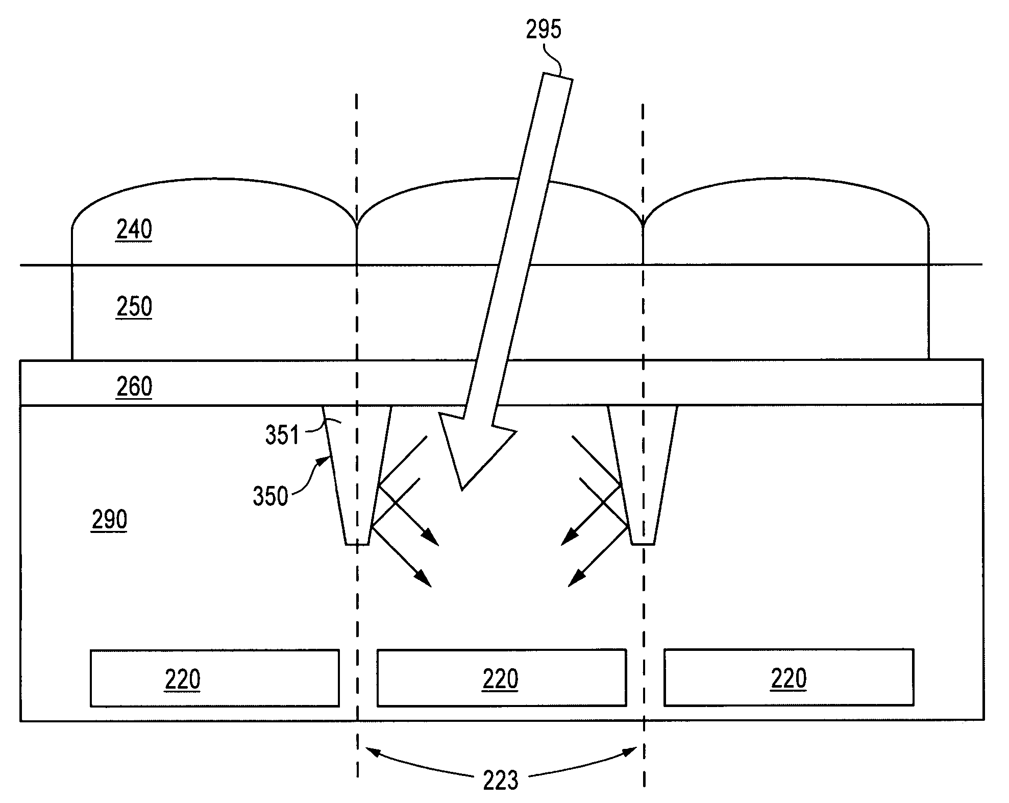
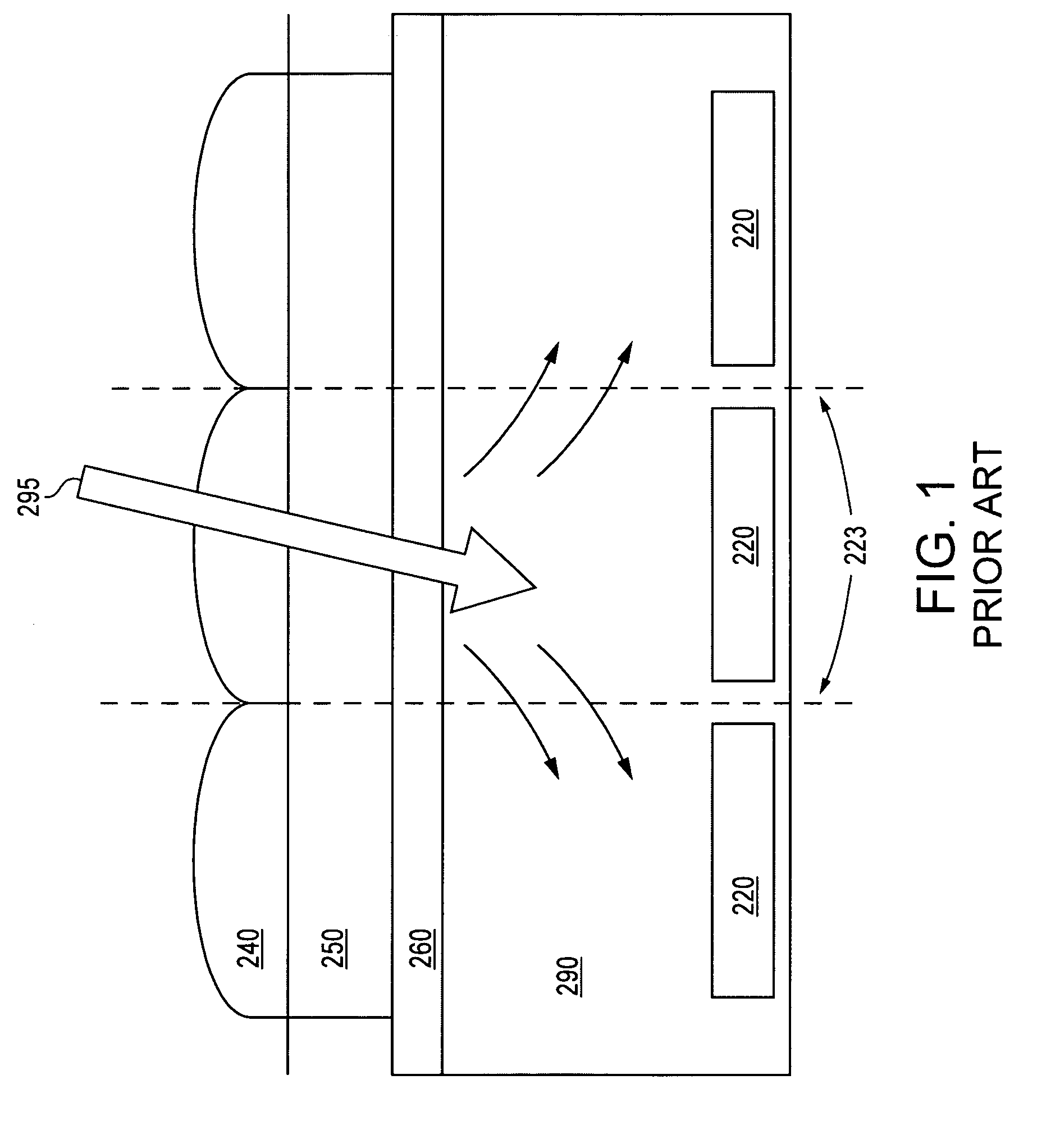
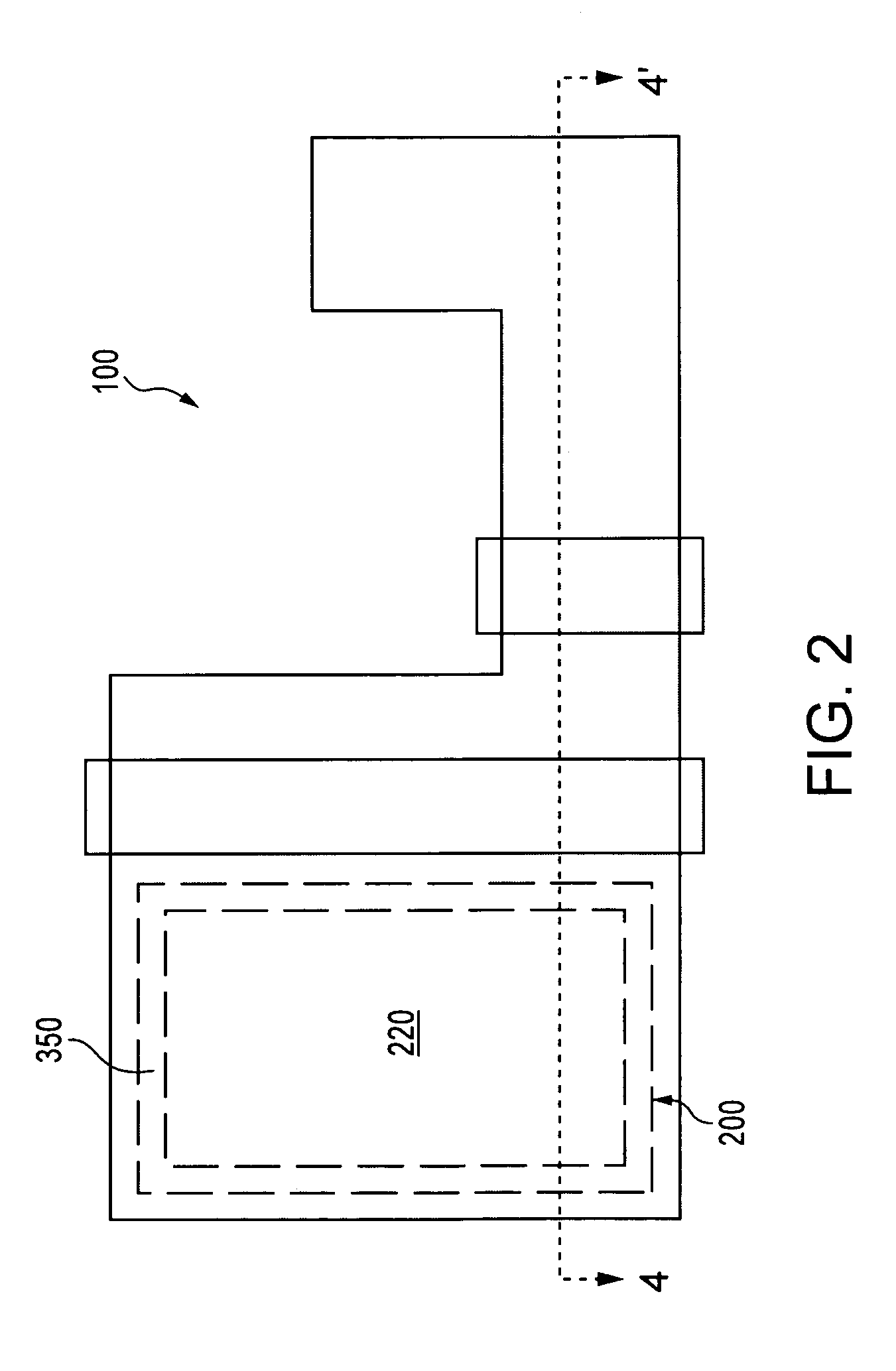
[0023]In the following detailed description, reference is made to the accompanying drawings which form a part hereof, and in which is shown by way of illustration specific embodiments by which the invention may be practiced. It should be understood that like reference numerals represent like elements throughout the drawings. These exemplary embodiments are described in sufficient detail to enable those skilled in the art to practice the invention. It is to be understood that other embodiments may be utilized, and that structural logical and electrical changes may be made without departing from the spirit and scope of the present invention.

[0024]The terms “wafer” and “substrate” are to be understood as including all forms of semiconductor wafers and substrates including silicon, silicon-on-insulator (SOI), silicon-on-sapphire (SOS), doped and undoped semiconductors, epitaxial layers of silicon supported by a base semiconductor foundation, and other semiconductor structures. Furthermo...


PUM


Abstract

A device and method for providing an optical trench structure for a pixel which guides incoming light onto the photosensor of the pixel. The optical trench structure has an optically reflecting barrier that substantially mitigates optical crosstalk. The optical trench structure is made of low dielectric constant material with an index of refraction that is less than the index of refraction of the material of surrounding layers (e.g., the substrate). This difference in refractive index causes an internal reflection into an optical path existing between a lens and pixel.

Description

FIELD OF THE INVENTION[0001]The invention relates generally to solid state imaging devices and more particularly to a method and structure for optically isolating pixel regions to reduce optical crosstalk in a solid state image sensor.BACKGROUND OF THE INVENTION[0002]There are a number of different types of semiconductor-based imagers, including charge coupled devices (CCD's), photodiode arrays, charge injection devices (CID's), hybrid focal plane arrays, and complementary metal oxide semiconductor (CMOS) imagers. Current applications of solid-state imagers include cameras, scanners, machine vision systems, vehicle navigation systems, video telephones, computer input devices, surveillance systems, auto focus systems, star trackers, motion detector systems, image stabilization systems, and other image acquisition and processing systems.[0003]CMOS imagers are well known. CMOS images are discussed, for example, in Nixon et al., “256×256 CMOS Active Pixel Sensor Camera-on-a-Chip,” IEEE ...

Claims


Application Information

Patent Timeline
Patent Type & Authority Patents(United States)
IPC IPC(8): H01L27/00H01L31/00H01L31/0232H01L31/062
CPCH01L27/1464H01L27/14629H01L27/1463H01L27/14627
Inventor LEE, JI SOOMOULI, CHANDRA
Owner APTINA IMAGING CORP
Why Eureka
Try Eureka