
Wiring substrate and radiation detector using same

a technology of wiring substrate and radiation detector, which is applied in the direction of radioation control devices, instruments, television systems, etc., can solve the problems of radiation damage to the signal processing element, degradation of reliability and lifetime of the radiation detector, etc., and achieve the effect of suppressing the degradation of reliability and lifetim

Inactive Publication Date: 2008-02-05
HAMAMATSU PHOTONICS KK
View PDF10 Cites 21 Cited by
  • Summary
  • Abstract
  • Description
  • Claims
  • Application Information

AI Technical Summary

Benefits of technology

The present invention provides a wiring substrate and a radiation detector that can suppress the transmission of radiation. The wiring substrate is made of a glass substrate with a conduction path for guiding an electric signal between the signal input surface and the signal output surface. The through hole in the glass substrate is designed so that the aperture in the predetermined plane is not on the extension of the aperture in the signal input surface. This configuration prevents the radiation from entering the signal processing element and degrading its reliability and lifetime. The radiation detector comprises the radiation detecting means, the wiring substrate section, and the signal processing means arranged in a predetermined alignment direction. The use of the wiring substrate with the conduction path can improve the reliability and lifetime of the radiation detector.

Problems solved by technology

In this connection, in a configuration wherein the scintillator, the photodetecting element array, the wiring substrate, and the signal processing element are arranged along a predetermined alignment direction, there arises a problem that the radiation having passed through the scintillator and others is incident through the wiring substrate into the signal processing element located downstream in the alignment direction.
This incidence of the radiation into the signal processing element will lead to radiation damage of the signal processing element and, in turn, to degradation of the reliability and lifetime of the radiation detector.

Method used


Image

  • Wiring substrate and radiation detector using same
  • Wiring substrate and radiation detector using same
  • Wiring substrate and radiation detector using same

Examples


Embodiment Construction

[0026]The preferred embodiments of the wiring substrate according to the present invention, and the radiation detector using it will be described below in detail with reference to the drawings. The same elements will be denoted by the same reference symbols in the description of the drawings, without redundant description. It is noted that dimensional ratios in the drawings do not always agree with those in the description.

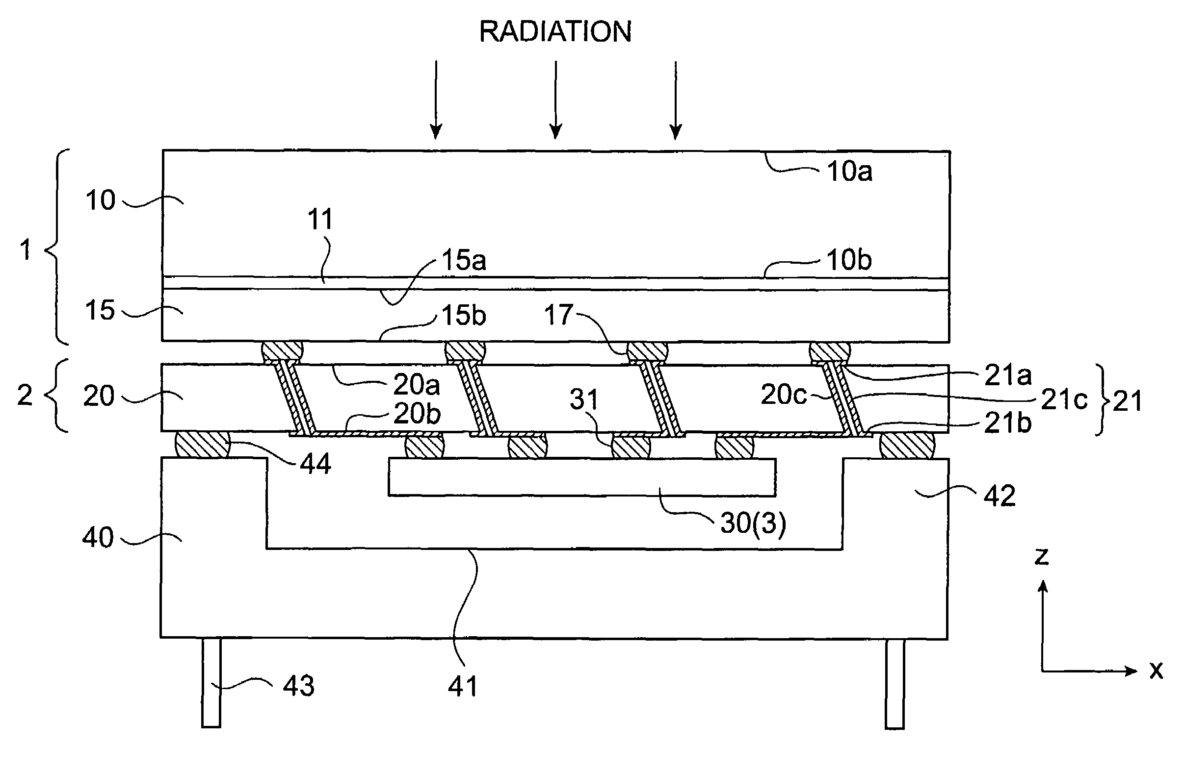
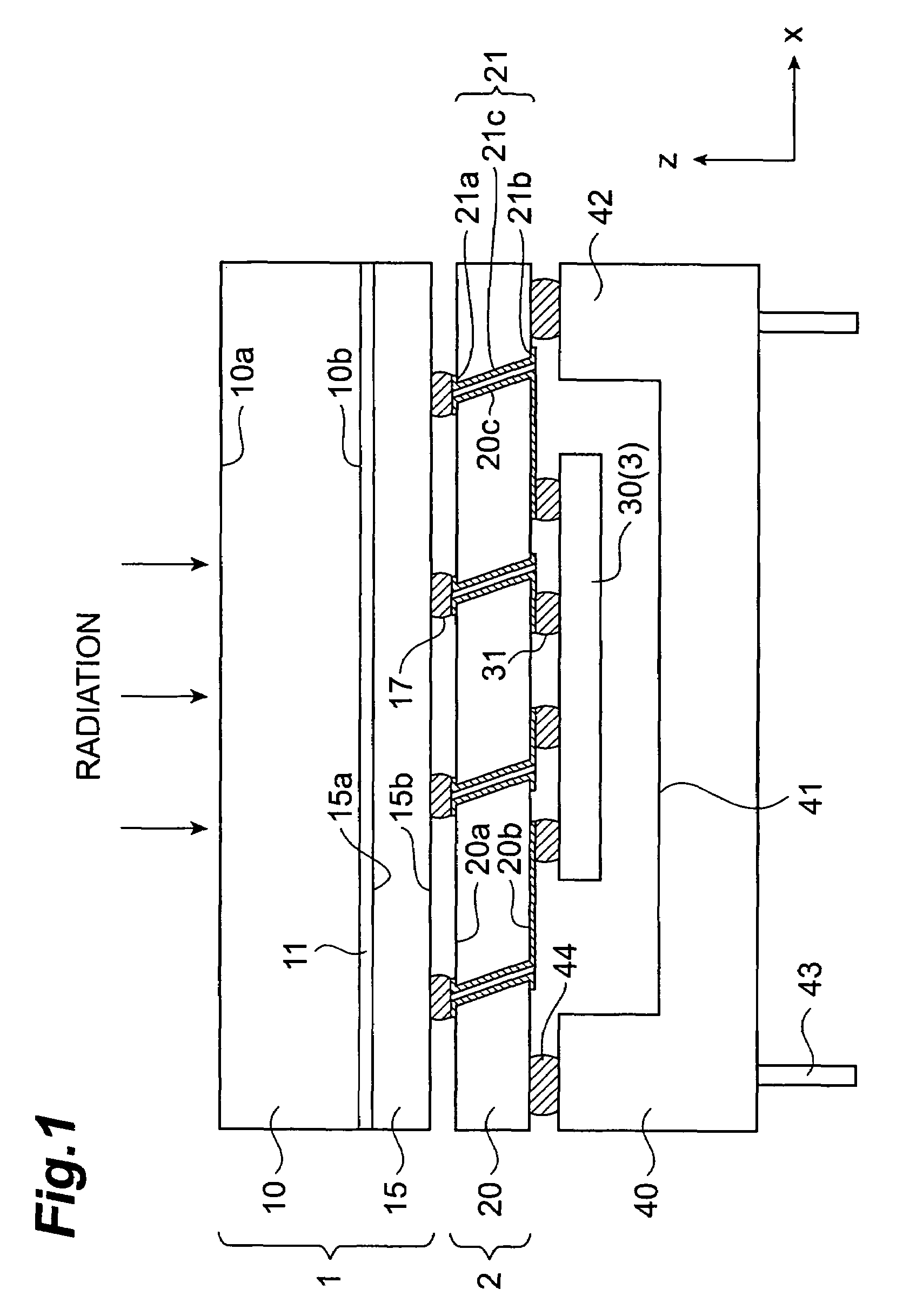
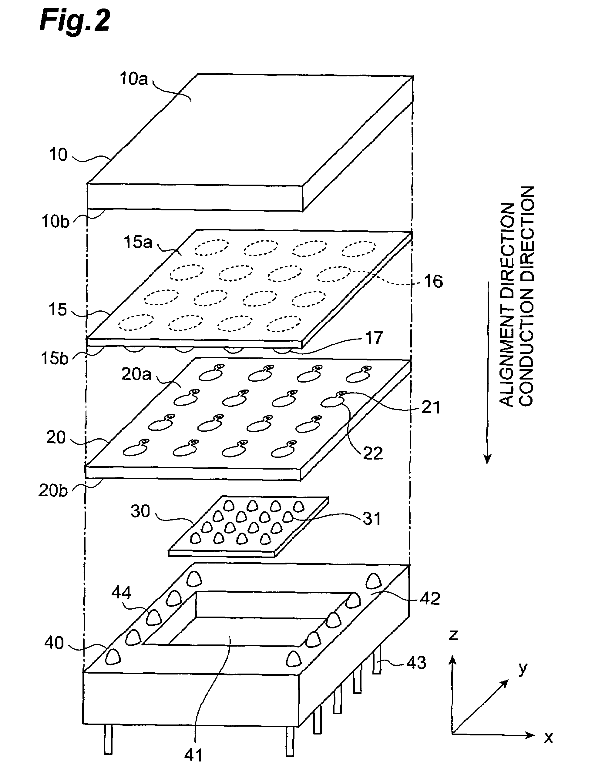
[0027]FIG. 1 is a sectional side view showing a sectional structure of an embodiment of the wiring substrate and the radiation detector according to the present invention. FIG. 2 is an exploded perspective view of components in the configuration of the wiring substrate and the radiation detector shown in FIG. 1. In each of the drawings hereinafter, an axis along a direction of incidence of radiation is defined as z-axis, and two axes perpendicular to this z-axis are defined as x-axis and y-axis, as shown in FIGS. 1 and 2, for the convenience of description. In thi...


PUM


Abstract

A wiring substrate section 2, which has a wiring substrate 20 with through holes 20c each filled with a conductive member 21 serving as a conduction path for guiding a detected signal, is installed between a radiation detecting section 1 comprised of a scintillator 10 and a PD array 15, and a signal processing element 30 for processing the detected signals outputted from the PD array 15. Each through hole 20c in the wiring substrate 20 is formed so that, with respect to a predetermined plane perpendicular to a conduction direction from an input surface 20a to an output surface 20b, an aperture of the through hole 20c in that plane is not on an extension along the conduction direction of an aperture of the through hole 20c in the input surface 20a and so that the through hole 20c cannot be seen through from the input surface 20a to the output surface 20b. This obtains the wiring substrate capable of suppressing transmission of radiation, and a radiation detector using it.

Description

TECHNICAL FIELD[0001]The present invention relates to a wiring substrate provided with conduction paths for guiding an electric signal, and a radiation detector using it.BACKGROUND ART[0002]As a radiation detector used for CT sensors and others, there is a detector of a configuration wherein, with respect to a semiconductor photodetecting element array such as a photodiode array, a scintillator is installed on a light-incident surface of the photodetecting element array. In the radiation detector of this type, when the radiation such as X-rays, γ-rays, or charged particles, which is an object to be detected, is made incident on the scintillator, the radiation generates scintillation light in the scintillator. Then the semiconductor photodetecting elements detect this scintillation light, thereby detecting the radiation.[0003]With respect to the photodetecting element array, a signal processing element is provided in order to perform signal processing of detected signals outputted fr...

Claims


Application Information

Patent Timeline
Patent Type & Authority Patents(United States)
IPC IPC(8): H01L31/00G01T1/20H01L23/48G01T1/24G01T7/00H01L27/14H01L27/146H01L31/0232H01L31/09H04N5/32H05K1/02H05K1/11H05K3/42
CPCH01L27/14618H01L27/14634H01L31/02322H01L2224/16225H05K1/115H05K3/42H05K1/02H01L27/146H01L31/02G01T1/24G01T1/20
Inventor SHIBAYAMA, KATSUMIKUSUYAMA, YUTAKAHAYASHI, MASAHIRO
Owner HAMAMATSU PHOTONICS KK
Learn More