Semiconductor device and driving method thereof

a technology of semiconductor devices and drives, applied in the field of digital circuits, can solve the problems of sequential malfunction in subsequent digital circuits, circuits that do not operate normally, and high possibility of malfunction, so as to prevent the delay in the operation of the transistor due to the gate capacitor

Inactive Publication Date: 2008-02-05
SEMICON ENERGY LAB CO LTD
View PDF35 Cites 22 Cited by
  • Summary
  • Abstract
  • Description
  • Claims
  • Application Information

AI Technical Summary

Benefits of technology

[0067]Meanwhile, when a circuit element includes a transistor and the corrected input signal is inputted to the gate of the transistor, a gate capacitor of the transistor is connected in series with a first capacitor element or a second capacitor element. Therefore, the resultant capacitance obtained by the seri

Problems solved by technology

In this case, the digital circuit does not operate normally, leading to a high possibility of malfunction.
Further, it can cause a sequential malfunction in the subsequent digital circuit.
In this case, the digital circuit does not operate normally, leading to a high possibility of a malfunction.
Further, it can cause a sequential malfunction at a subsequent digital circuit.
However, when the binary potentials VDD′ and VSS′ of the input signal IN are in the relations of VDD′VSS respectively, the output signal OUT having a desired potential is not obtained, thereby the inverter may not operate normally.
That is, when the binary potential of the input signal IN is out of the predetermined range, the circuit elements of the digital circuit malfunction.
Therefore, the output signal OUT having a desired potential can not be obtained and the digital circuit does not function normally.
A potential of the input signal supplied from a circuit or a wiring of a prior stage is not always an appropriate value for operating the digital circuit normally.
However, a high-speed operation of the semiconductor device is frequently hindered by using the level shifter, because level shifters generally have disadvantag

Method used


Image

  • Semiconductor device and driving method thereof
  • Semiconductor device and driving method thereof
  • Semiconductor device and driving method thereof

Examples


embodiment mode 1

[0091]In this embodiment mode, a specific configuration and an operation of an inverter as an example of the digital circuits of the invention are described.

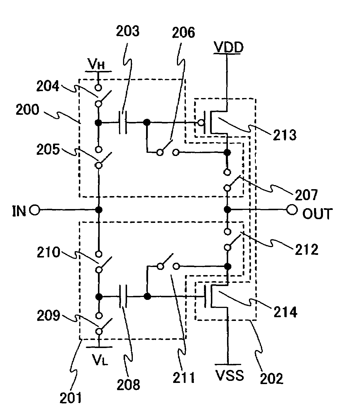
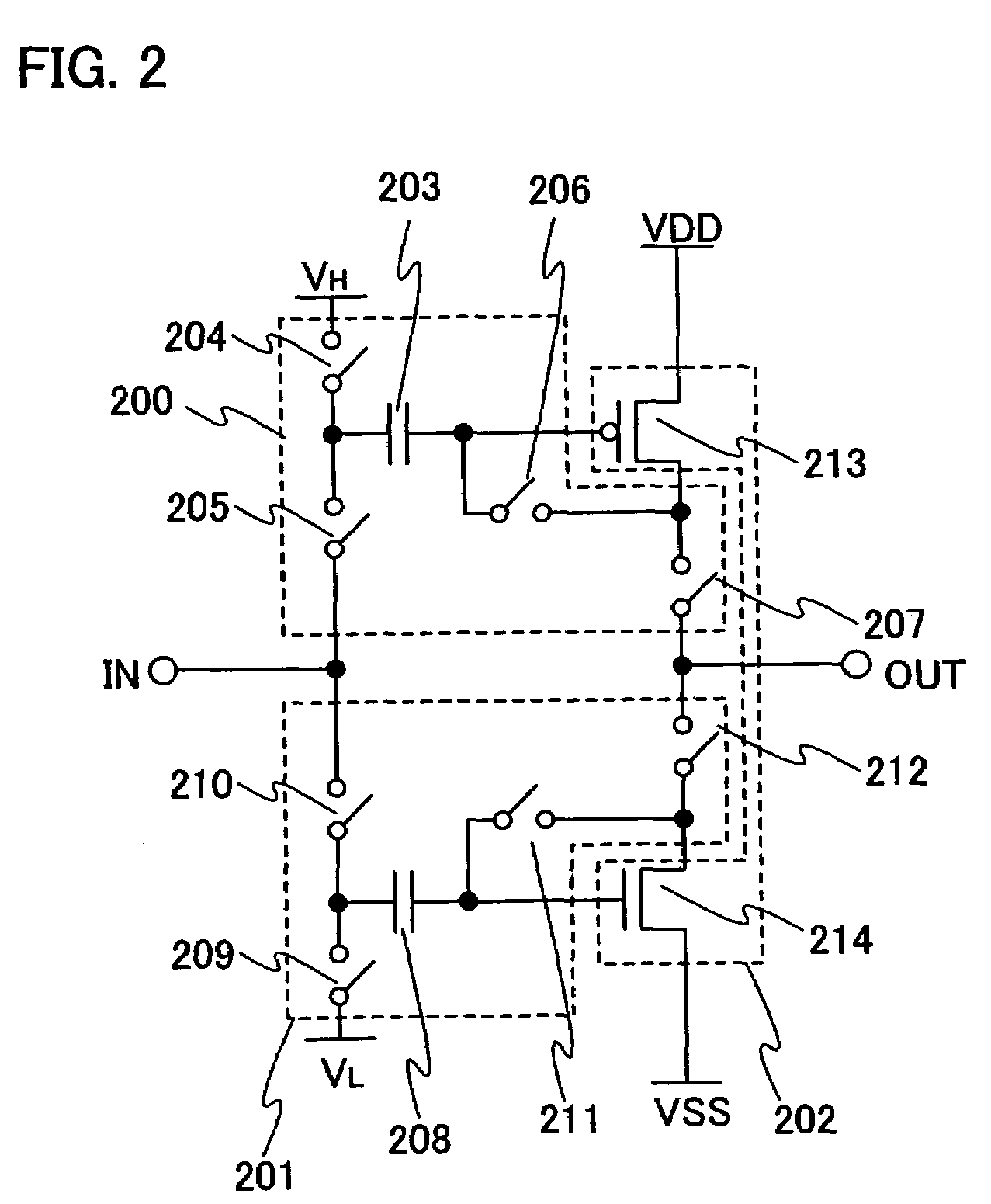
[0092]FIG. 2 shows a configuration of an inverter of this embodiment mode. Reference numerals 200 and 201 denote correcting units and reference numeral 202 denotes a circuit element group.

[0093]The correcting unit 200 includes a first capacitor element 203 and 4 switches 204 to 207 for controlling a potential supply to the first capacitor element 203. Meanwhile, the correcting unit 201 includes a second capacitor element 208 and 4 switches 209 to 212 for controlling the potential supply to the second capacitor element 208.

[0094]The switch 205 controls a supply of a potential of an input signal to a first electrode of the first capacitor element 203. The switch 204 controls a supply of a power source potential on the high potential side VH to the first electrode of the first capacitor element 203. The switch 206 controls a connec...

embodiment mode 2

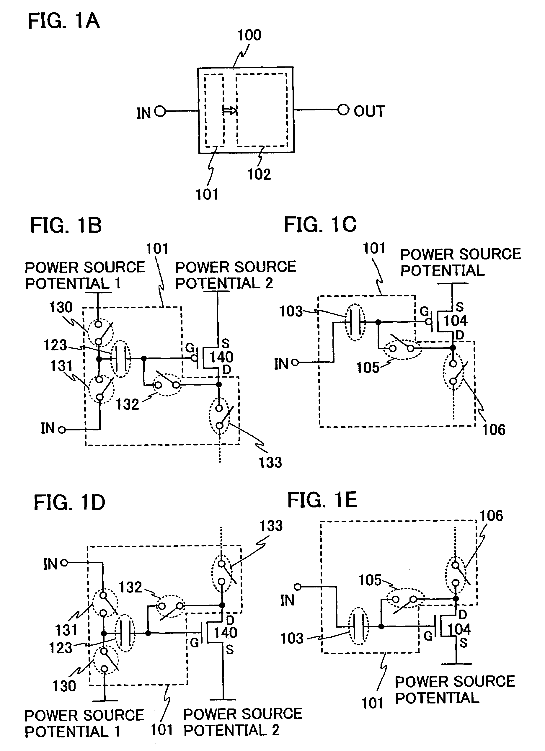
[0123]Hereinafter explained is the case where the inverter as shown in embodiment mode 1 is used as a clocked inverter. Regarding the inverter hereof, a signal with the same amplitude as that of the power source is inputted as a clock signal which is to be inputted to gates of the transistor 212 and a transistor 222, and a signal with a small amplitude is inputted as the input signal IN. Shown in this embodiment mode is a case where the configurations shown in FIGS. 1B and 1D are applied.

[0124]In the correcting unit of the digital circuit of the invention, a switch for controlling a potential supply to a drain of the transistor of which the gate is connected to a second electrode of a capacitor element among the transistors in the circuit element is provided. However, when there is already a switch which controls the potential supply to the drain of the transistor in circuit elements other than a correction unit, the switch may be a substitute for the former switch.

[0125]Shown in FI...

embodiment mode 3

[0137]In this embodiment mode, a different configuration of the inverter which is one example of the digital circuits according to the invention from that described in the embodiment mode 1 will be described. The configurations shown in FIGS. 1C and 1E are applied to this embodiment mode.

[0138]A configuration of an inverter of the embodiment mode will be shown in FIG. 6. Reference numerals 301 and 302 denote correcting units and reference numeral 303 denotes a circuit element group.

[0139]The correcting unit 301 includes a first capacitor element 304 and two switches 306 and 307 for controlling the potential supply to the first capacitor element 304. The correcting unit 302 includes a second capacitor element 305 and two switches 308 and 309 for controlling the potential supply to the second capacitor element 305.

[0140]The switch 306 controls a connection between a gate and a drain of a p-channel type transistor 310. The gate thereof is connected to a second electrode of the first ca...


PUM


Abstract

It is an object of the invention to provide a digital circuit which can operate normally regardless of binary potentials of an input signal. A semiconductor device having a correcting unit and a logic unit wherein the correcting unit includes a capacitor, first and second switches, wherein the first electrode of the capacitor is connected to the input terminal and the second electrode of the capacitor is connected to the gate of the transistor in the logic circuit, wherein the first switch controls the connection between a gate and drain of the transistor and the second switch controls the potential to be supplied to the drain of the transistor is provided.

Description

BACKGROUND OF THE INVENTION[0001]1. Field of the Invention[0002]The present invention relates to a digital circuit which operates in synchronism with a digital signal, and more particularly to a semiconductor device having a single or a plurality of the digital circuits and a driving method thereof.[0003]2. Description of the Related Art[0004]A logic circuit processing a digital signal (hereinafter referred to as a digital circuit) is configured with a single or a plurality of logic elements as a basic unit. The logic element is a circuit which provides one output corresponding to a single or a plurality of inputs. Examples of the logic elements include an inverter, an AND, an OR, a NOT, a NAND, a NOR, a clocked inverter, and a transmission gate and the like.[0005]The logic element is configured with a single or a plurality of circuit elements such as transistors, resistors and capacitor elements. By operating the plurality of circuit elements in accordance with a digital signal inp...

Claims


Application Information

Patent Timeline
IPC IPC(8): H03K19/0175H03K19/017
CPCH03K19/01728
Inventor KIMURA, HAJIME
Owner SEMICON ENERGY LAB CO LTD
Why Eureka
Try Eureka