Reduction of voltage spikes in switching half-bridge stages

Active Publication Date: 2008-03-06
TEXAS INSTR INC
View PDF4 Cites 25 Cited by
  • Summary
  • Abstract
  • Description
  • Claims
  • Application Information

AI Technical Summary

Benefits of technology

[0012]In accordance with the present invention, there is provided a system and method for configuring a switching half bridge in an amplifier to take advantage of component characteristics to slow a switching speed of a power switch to avoid high voltage spikes. According to an exemplary embodiment of the present invention, internal components such as parasitic bond wire inductances are arranged in conjunction with power switch driver power paths to impact a gate voltage to slow a switching speed of a power switch. The bond wire paths for a half bridge power switch are arranged to obtain separate component values for a

Problems solved by technology

If the switching events occur very rapidly, the switched current can produce high voltage spikes that can exceed the ratings of circuit 10, and damage or destroy MOSFETs 13, 14.
However, in audio applications with a rapidly changing continuous input, slowing switching speed can have a negative impact on application performance.
If switching speed is reduced, for example, in an audio application, the resulting impact on performance tends to increase the total harmonic distortion (THD) or increase shoot through currents by limiting dead time response.
The

Method used


Image

  • Reduction of voltage spikes in switching half-bridge stages
  • Reduction of voltage spikes in switching half-bridge stages
  • Reduction of voltage spikes in switching half-bridge stages

Examples


Embodiment Construction

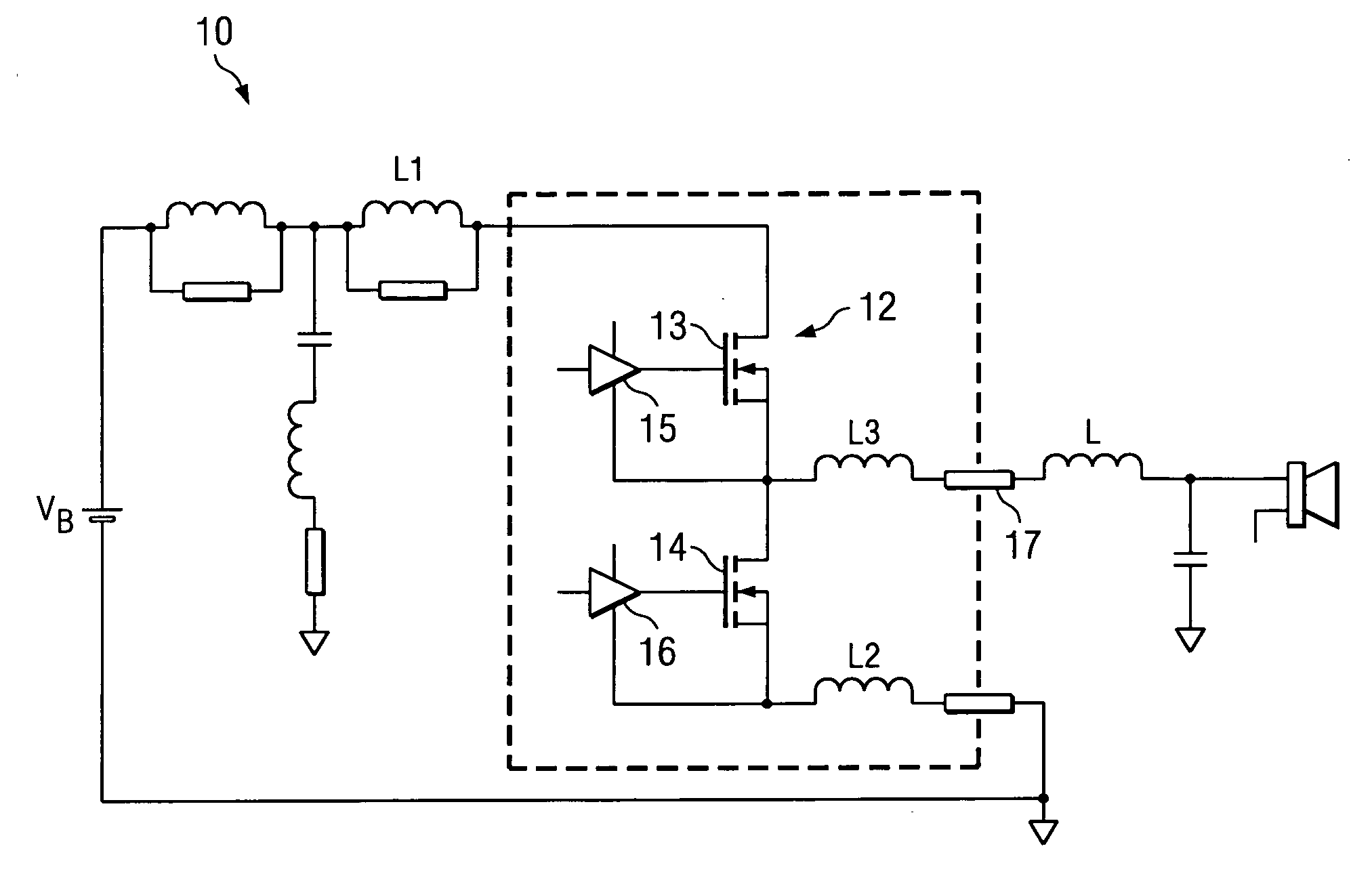
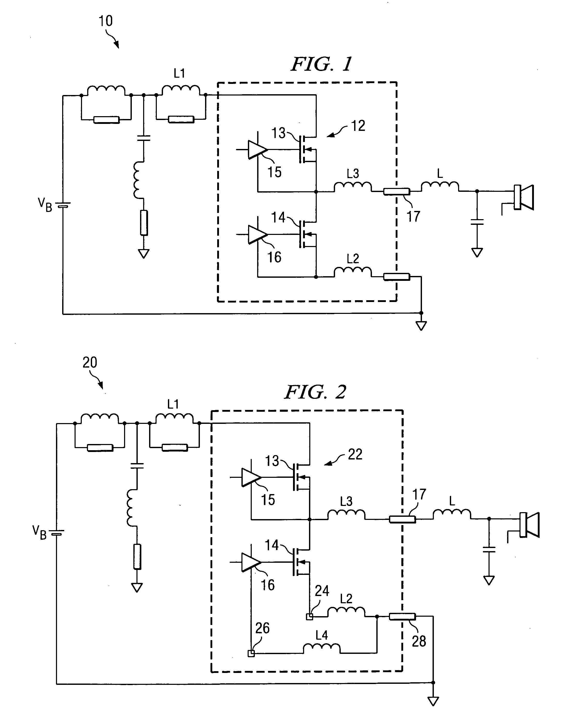
[0021]Referring to FIG. 1, a typical class D audio amplifier is illustrated generally as circuit 10. A number of inherent characteristics of circuit 10 are modeled as parasitic impedances, including an inductances L2-L3 related to bond wire inductance, and inductor L1 related to traces on a printed circuit board (PCB). Switches 13, 14, illustrated as FETs in circuit 10 can be exposed to high voltage spikes during switching events, especially when switches 13, 14 are switched rapidly. For example, in the state where switch 13 is not conducting and switch 14 is conducting, current can flow from output inductor L through output pin 17 and through switch 14 to ground. In this state, when switch 14 turns off, the current supplied by inductor L begins to flow through inductor L3 and the body diode of switch 13, and is input into inductor L1. Inductor L1 is modeled as a parasitic inductance, which is maintained at as low a value as possible due to its impact on the generation of high volta...


PUM


Abstract

A path configuration for a power switch and driver can introduce independent parasitic inductance coupled to the power switch to slow a switching speed of the switch and reduce voltage spikes on the switch during switching events. The path for low side supply of the drive to the negative DC voltage reference is separate from the path of the power switch to the reference. The resulting reduction in voltage spikes due to the slowed switching time maintains performance in an audio amplifier without modifying a switch command signal to compensate for voltage spikes. The path configuration avoids reliance on specifying higher rated components that increase application costs.

Description

CROSS REFERENCE TO RELATED APPLICATIONS[0001]N / ASTATEMENT REGARDING FEDERALLY SPONSORED RESEARCH OR DEVELOPMENT[0002]N / ABACKGROUND OF THE INVENTION[0003]1. Field of the Invention[0004]The present relates generally to performance improvements in switching circuits and relates more particularly to a reduction in voltage spike magnitude appearing across power switches in a switched power application.[0005]2. Description of Related Art[0006]Class D audio amplifiers have a number of advantages including high efficiency and low cost. A portion of a power stage for an amplifier is illustrated in FIG. 1 as circuit 10. Circuit 10 includes a switching half bridge 12 composed of MOSFETs 13 and 14. In the case of an audio amplifier application, switches 13 and 14 are switched in accordance with a PWM signal related to an input audio signal. Where circuit 10 is used in a high power application such as for a loud speaker, a supply voltage maximum is limited in some cases by a voltage rating of po...

Claims


Application Information

Patent Timeline
IPC IPC(8): H03F3/217
CPCH03F1/342H03F1/52H03F1/523H03F3/2171H03K17/6871H03F2200/03H03F2200/117H03F2200/351H03K17/166H03F3/2173
Inventor UNNIKRISHNAN, SREENATHTSECOURAS, MIKEBERWICK, JEFF
Owner TEXAS INSTR INC
Why Eureka
Try Eureka