Manufacturing method of groove-type super junction device

A manufacturing method and super-junction technology, applied in semiconductor/solid-state device manufacturing, semiconductor devices, electrical components, etc., can solve problems such as difficulty in improving epitaxial filling process, affecting production yield, and increasing reverse leakage current of devices, so as to achieve improvement The effect of EMI performance

Active Publication Date: 2016-06-08
SHANGHAI HUAHONG GRACE SEMICON MFG CORP
View PDF6 Cites 6 Cited by
  • Summary
  • Abstract
  • Description
  • Claims
  • Application Information

AI Technical Summary

Problems solved by technology

[0003] The biggest difficulty of this process is to fill the trench with silicon epitaxy. The existing manufacturing method is very easy to cause a sharp increase in the reverse leakage current of the device, which will lead to the failure of the device and seriously affect the production yield.
In addition, the epitaxial filling process itself is very difficult to improve, so how to overcome the impact of the epitaxial filling process itself on the super junction device is the main problem of the present invention.

Method used


Image

  • Manufacturing method of groove-type super junction device
  • Manufacturing method of groove-type super junction device
  • Manufacturing method of groove-type super junction device

Examples


Embodiment Construction

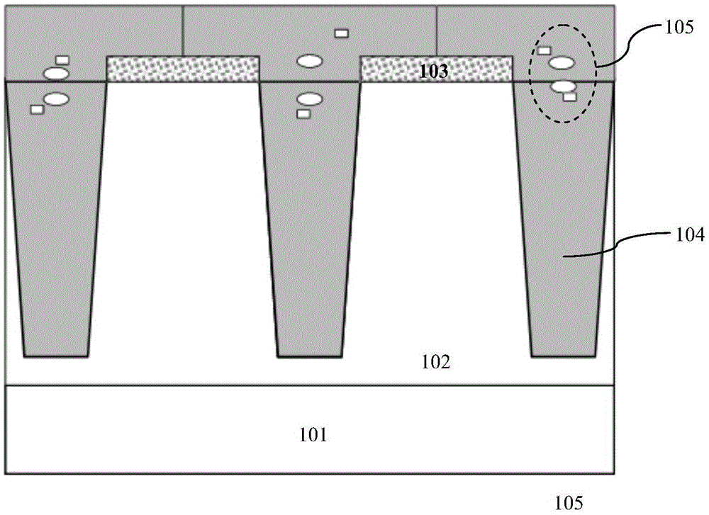
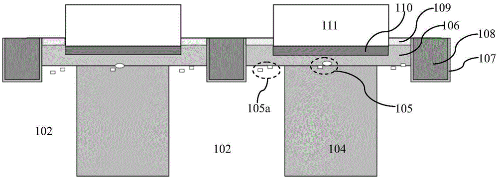
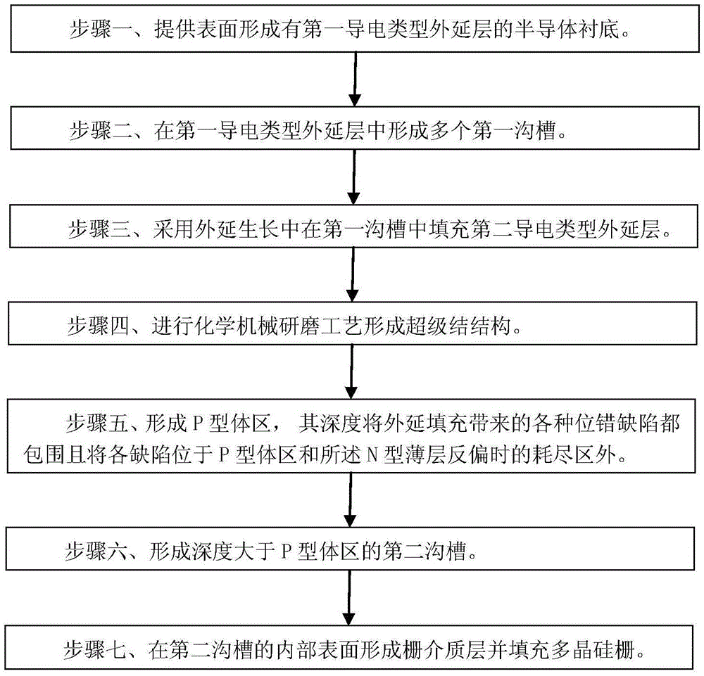
[0047] Firstly, the problems of existing trench superjunction manufacturing methods are introduced, such as figure 1 Shown is a schematic diagram of the structure of the super junction formed by the manufacturing method of the existing trench type super junction device; the existing method includes the following steps:

[0048] Step 1: Provide a semiconductor substrate such as a silicon substrate 101 , and an N-type epitaxial layer such as an N-type silicon epitaxial layer 102 is formed on the surface of the semiconductor substrate 101 .

[0049] Step 2: Forming a plurality of trenches in the N-type epitaxial layer 102 by photolithography. The hard mask layer 103 is used when etching the trench.

[0050] Step 3: filling the trench with a P-type epitaxial layer such as a P-type silicon epitaxial layer 104 during epitaxial growth, and the P-type epitaxial layer 104 will simultaneously extend to the surface of the N-type epitaxial layer 102 outside the trench.

[0051] Depend o...


PUM

PropertyMeasurementUnit
thicknessaaaaaaaaaa
thicknessaaaaaaaaaa
thicknessaaaaaaaaaa

Abstract

The invention discloses a manufacturing method of a groove-type super junction device. The method comprises the steps of: providing a semiconductor substrate, wherein a first conductive type epitaxial layer is formed on the surface; forming a plurality of first grooves in the first conductive type epitaxial layer; filling the first grooves with a second conductive type epitaxial layer in an epitaxial growth process; carrying out a chemical and mechanical grinding process to form a super junction; forming a P type body area on the surface of the super junction, wherein the depth of the P type body area meets the requirements that all kinds of crystal lattice defects caused by epitaxial filling are surrounded, and each defect is arranged outside a depletion area of the reverse bias process of the P type body and an N type film layer; forming a second groove whose depth is larger than the P type body area; and forming a gate medium layer on the bottom surface and the side surface of the second groove, and filling the second groove with polysilicon grids. According to the invention, the negative influences caused by the epitaxial filling process on the super junction device are avoided, the reverse leakage current of the super junction device is reduced, and the production yield rate of the super junction device is improved; in addition, parasitic capacitance is reduced, and the electromagnetic interference performance of the circuit and the system is improved.

Description

technical field [0001] The invention relates to a manufacturing process method of a semiconductor integrated circuit, in particular to a manufacturing method of a trench type super junction device. Background technique [0002] The super junction is composed of alternately arranged P-type thin layers and N-type thin layers formed in the semiconductor substrate. The existing super junction manufacturing method includes the manufacturing method of the trench type super junction device. This method is through the trench To make a super junction by trench technology, it is necessary to etch a trench with a certain depth and width on the N-type doped epitaxial layer on the surface of a semiconductor substrate such as a silicon substrate, and then use the method of epitaxial filling (ERIFilling) to fill the etched trench. P-type doped silicon epitaxy is filled on the top, and the filling area is required to have a complete crystal structure, so that high-performance devices can be...

Claims


Application Information

Patent Timeline
Patent Type & Authority Applications(China)
IPC IPC(8): H01L29/06H01L21/20H01L21/306H01L21/265
CPCH01L21/02365H01L21/20H01L21/265H01L21/30625H01L29/0603H01L29/0684
Inventor 李昊
Owner SHANGHAI HUAHONG GRACE SEMICON MFG CORP
Why Eureka
Try Eureka