
Coherent optical detector and coherent communication system and method

a detector and coherent technology, applied in the field of integrated electrooptical receiving devices, can solve the problems of low-cost receivers, inability to implement, and increase the complexity of receivers in coherent detection schemes

Inactive Publication Date: 2008-02-05
CELIGHT
View PDF14 Cites 43 Cited by
  • Summary
  • Abstract
  • Description
  • Claims
  • Application Information

AI Technical Summary

Benefits of technology

The solution enables efficient demodulation of complex optical signals, reducing costs and complexity by integrating components on a single chip, improving performance and stability, and allowing for simultaneous phase and amplitude measurement, thus enhancing communication and sensing applications.

Problems solved by technology

Such communication schemes were abandoned in the late 1980's and are still not implemented due to their complexity and high cost.
The cost is increased complexity of receivers in coherent detection schemes.
The main problem is related to the development of compact, reliable, and low-cost receivers for such advanced modulating schemes.
There are no completely planar integrated solutions for the device that are capable to provide an arbitrary format demodulation (phase and / or amplitude modulation).

Method used


Image

  • Coherent optical detector and coherent communication system and method
  • Coherent optical detector and coherent communication system and method
  • Coherent optical detector and coherent communication system and method

Examples


Embodiment Construction

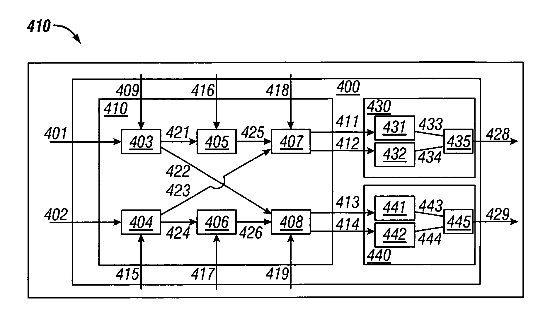
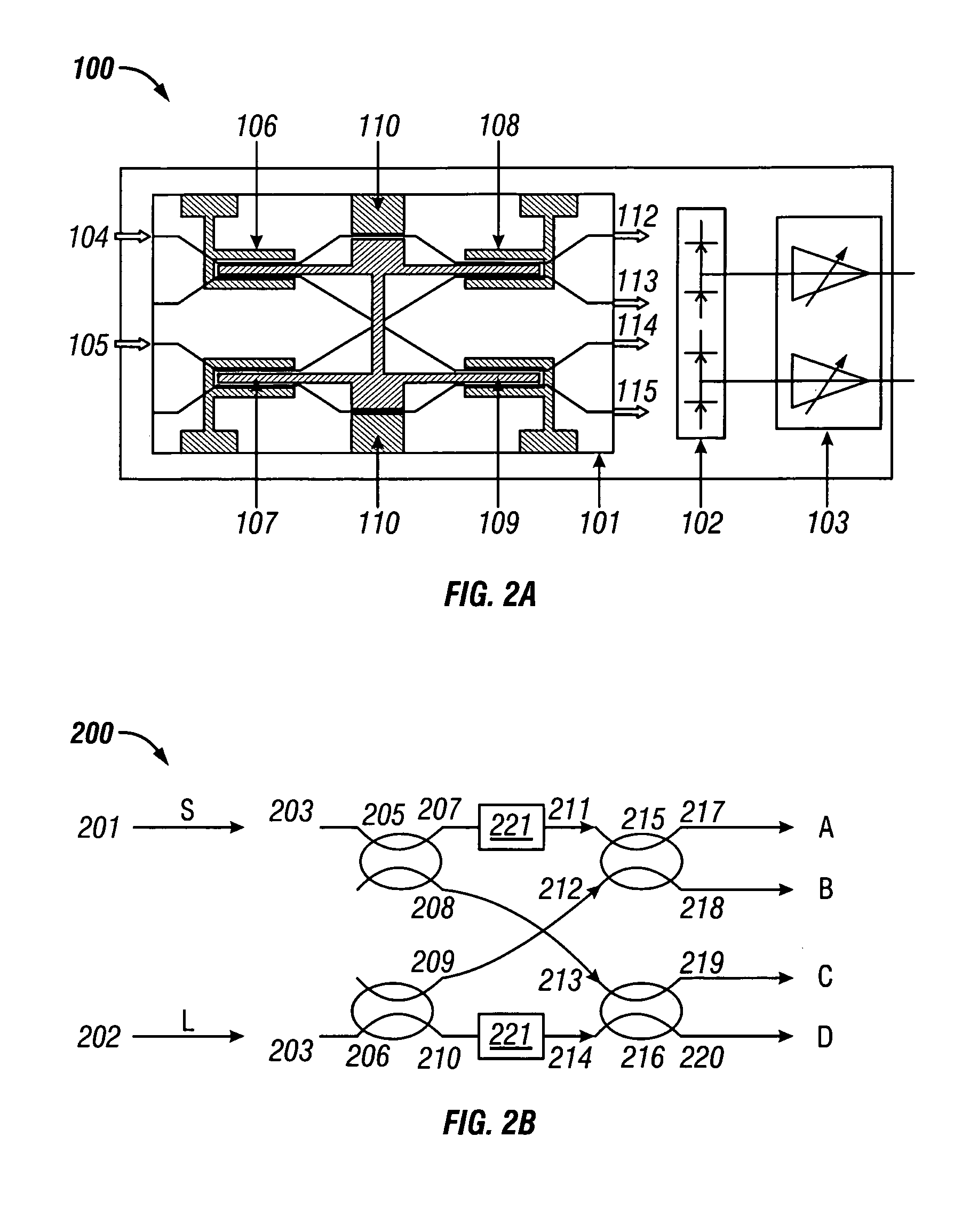
[0042]In one embodiment of the present invention, an optical device, such as optical device 200 illustrated in FIG. 2(a), hereafter the “Optical Device”, is provided that includes a first device input, and a second device input, first, second, third and fourth couplers (mixers) and first, second, third and fourth device outputs. Each coupler includes two adjacent waveguides providing the mixing of the optical signals propagating in these adjacent waveguides. The first and second device inputs both are connected, respectively, to the first coupler and the second coupler.

[0043]One output of the first coupler is connected to one input of the third coupler while another output of the first coupler is connected to the one input of the fourth coupler. An output of the second coupler is connected to another input of the fourth coupler while another output of the first coupler is connected to another input of the third coupler. The Optical Device further includes two crossing waveguides, wh...


PUM

PropertyMeasurementUnit
spacingaaaaaaaaaa
spacingaaaaaaaaaa
frequencyaaaaaaaaaa

Abstract

An optical device is provided with first and second inputs. A first coupler coupled is coupled to the first input and produces at least a first and second output. A second coupler is coupled to the second input and produces at least a first and second output. A third coupler is coupled to the first output of the first coupler and to the first output of the second coupler. A fourth coupler is coupled to the second output of the first coupler and to the second output of the second coupler. First and second crossing waveguides are provided with an angle selected to minimize crosstalk and losses between the first and second cross waveguides. The first crossing waveguide connects one of the first or second outputs from the first coupler with an input of the fourth coupler. The second crossing waveguide connects one of the first or second outputs from the second coupler with an input of the third coupler. A first phase shifter is coupled to the first and second waveguides. The first and second waveguides connect one of the outputs of the first or second coupler and one of the inputs of the third or fourth couplers. The first, second, third and fourth couplers, the two crossing waveguides and the phase shifter are each formed as part of a single planar chip made of an electro-optical material.

Description

CROSS-REFERENCE TO RELATED APPLICATIONS[0001]This application claims the benefit of Ser. No. 60 / 462,348 filed Apr. 11, 2003, and is also a continuation-in-part of Ser. Nos. 09 / 962,243 filed Sep. 26, 2001 now U.S. Pat. No. 7,167,651 and 10 / 613,772 filed Jul. 2, 2003, all of which applications are fully incorporated herein by reference.FIELD OF THE INVENTION[0002]This invention relates generally to integrated electro-optical receiving device and their methods and use, and more particularly to electro-optical receiving devices formed on a single chip, and their methods of use, as well as optical communications systems and methods that utilize their coherent detection.BACKGROUND OF THE INVENTION[0003]Lasers are widely used today in fiber and free space segments for high data rate communication links, remote sensing applications (LIDAR) and more. In these applications the modulated light signal is modulated using electro-optical modulators and demodulated using, usually, electro-optical ...

Claims


Application Information

Patent Timeline
Patent Type & Authority Patents(United States)
IPC IPC(8): G02B6/12G02B6/26G02F1/03G02F1/07H04B10/06G02BH04B10/148H04B10/155H04B10/18H04J14/00H04J14/02
CPCG02B6/12004G02B6/12007H04B10/50H04B10/60H04B10/61H04B10/613H04B10/614H04B10/6162H04B10/63H04J14/005G02B2006/12147H04J14/02
Inventor SHPANTZER, ISAACKAPLAN, ARKADYSALAMON, AVIVACHIAM, YAAKOVKHURGIN, JACOB B.TSEYTLIN, MICHAELCHO, PAK SHINGGREENBLATT, ARTHURKERR, CHRISTOPHERHARSTON, GEOFFREY
Owner CELIGHT
Learn More