Organic EL display device

a display device and organic material technology, applied in the direction of discharge tube luminescnet screen, discharge tube main electrode, discharge tube/lamp details, etc., can solve the problem of reducing the light-emitting area of organic materials used as bank materials, and reducing the light-emitting area. , to achieve the effect of suppressing the light-emitting region

Inactive Publication Date: 2008-02-19
SAMSUNG DISPLAY CO LTD +1
View PDF12 Cites 22 Cited by
  • Summary
  • Abstract
  • Description
  • Claims
  • Application Information

AI Technical Summary

Benefits of technology

[0019]The present invention has been made in view of the above-mentioned circumstances and it is an object of the present invention to provide an organic EL display device which suppresses the degradation of the light emitting region which is attributed to a bank film and, at the same time, can suppress the failure in formation of a counter electrode and a light emitting material layer and the failure in image display.

Problems solved by technology

The light emitting material layer (organic material layer), due to the unexpected diffusion of moisture, oxygen and the like in the inside thereof, inevitably receives the change of electron state and loses desirable electric field light-emitting characteristics.
With respect to such a drawback, it is unavoidable that any organic material which is used as the bank material contains approximately 0.1% of water content.
Accordingly, so long as the bank film is formed of the organic material, it is difficult to prevent the occurrence of the non-light-emitting region at the end portion of the pixel which constitutes the organic EL element.
Further, even when an electron-transporting layer or a hole-transporting layer is formed between the bank film and the light emitting material layer, this does not solve this drawback.
The inventors have focused their attention on a shape of the bank film as a cause which generates such a drawback even with respect to the organic EL display device provided with the bank film made of inorganic material.

Method used


Image

  • Organic EL display device
  • Organic EL display device
  • Organic EL display device

Examples


embodiment 1

>

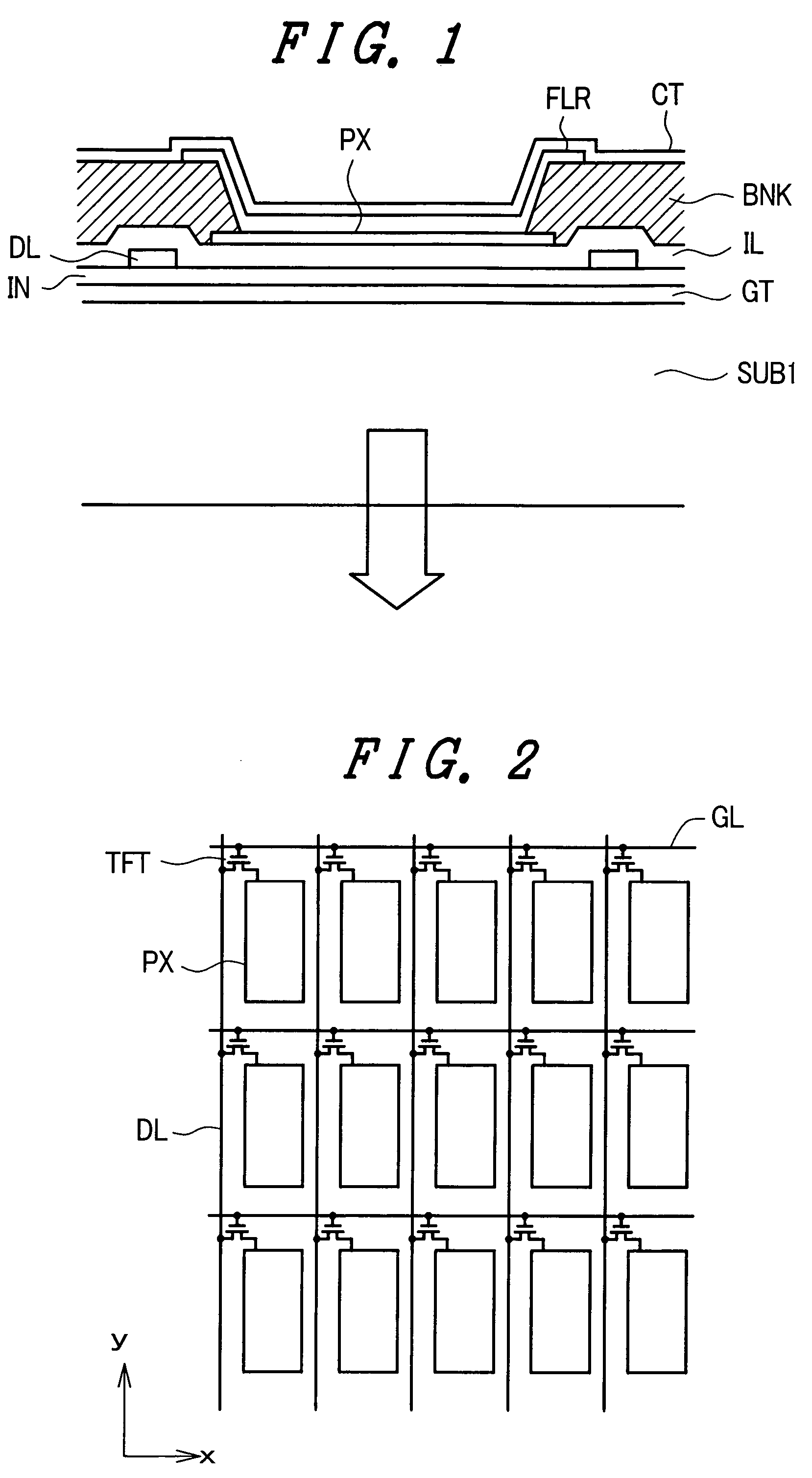
[0069]FIG. 2 is an equivalent circuit diagram of one embodiment of the organic EL display device according to the present invention.

[0070]In the drawing, gate signal lines GL which extend in the x direction in the drawing and are arranged in parallel in the y direction in the drawing and drain signal lines DL which extend in the y direction in the drawing and are arranged in parallel in the x direction in the drawing are formed.

[0071]Respective rectangular regions which are surrounded by these gate signal lines GL and drain signal lines DL constitute pixel regions and a mass of these pixel regions form a display region.

[0072]Each pixel region includes a thin film transistor TFT which is turned on in response to a scanning signal from the one-side (upper side in the drawing) gate signal line GL and a pixel electrode PX to which a video signal is supplied from the one-side (left side in the drawing) drain signal line DL by way of the thin film transistor TFT. In a current-drive type ...

embodiment 2

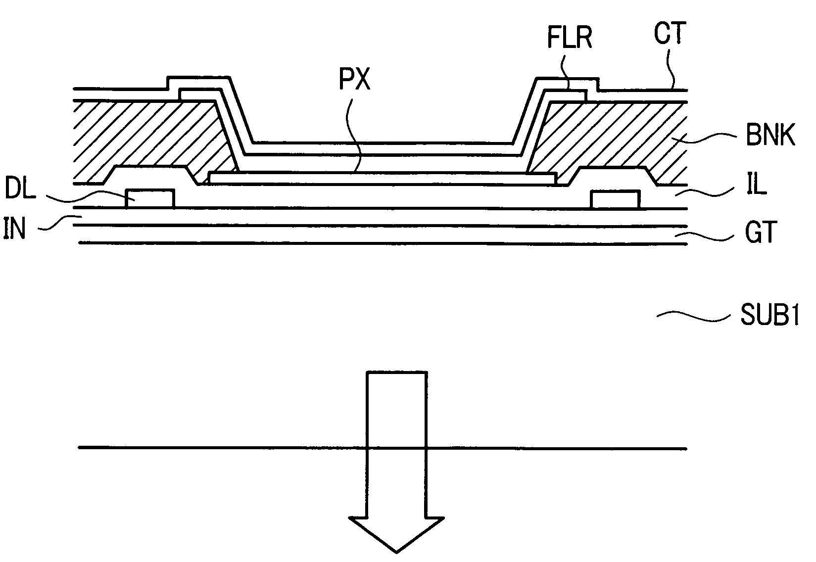
[0114]FIG. 7A to FIG. 7C are cross-sectional views respectively showing another embodiments of the side wall of the opening portion of the bank film BNK.

[0115]In providing the inclination of less than 85 degrees with respect to the principal surface of the substrate SUB1 (or the upper surface of the pixel electrode PX which is in contact with the bank film BNK as shown in FIG. 1 and FIG. 4) to the opening portion of the bank film BNK, due to conditions of wet etching or the dry etching, there may be a case that the side wall of the bank film BNK makes an angle of 85 degrees or more with respect to the principal surface of the substrate SUB1. In all of FIG. 7A to FIG. 7C, the side wall of the bank film BNK makes an angle of 85 degrees or more with respect to the principal surface of the substrate SUB1 in a region close to an tipper surface of the bank film BNK. Further, in FIG. 7C, the side wall of the bank film BNK bends backward toward the opening of the bank film BNK by making an ...

embodiment 3

[0119]FIG. 8A to FIG. 8D are cross-sectional views respectively showing another embodiments of the side wall of the opening portion of the bank film BNK.

[0120]Since the inclined surface of the side wall of the opening portion of the bank film BNK is formed by making use of the difference in the etching rate among respective layers of the bank film BNK as described above, it is a rare case that the side wall is formed as a straight flat face and it is often a case that the side wall is formed in a curved shape as shown in FIG. 8A to FIG. 8D. In FIG. 8A and FIG. 8D, a portion of the side face of the bank film BNK which is in contact with the principal surface of the substrate SUB1 (or a tangent or a contact flat face which is in contact with the portion) makes an angle of 85 degrees or more with respect to the principal surface of the substrate SUB1. In FIG. 8B and FIG. 8D, a portion of the side face of the bank film BNK in the vicinity of the upper surface of the bank film BNK (or a ...


PUM


Abstract

In an organic EL display device comprising a substrate, a plurality of pixel regions in each of which a first electrode, a light emitting material layer, and a second electrode are laminated in this order above the substrate, and a bank film formed above the substrate to separate respective one of the pixel regions from another of the pixel regions adjacent thereto, wherein the bank film has a plurality of openings exposing upper surfaces of the first electrodes to the light emitting material layers in the respective pixel regions, and the second electrode is formed over the a plurality of openings of the bank film in common with the pixel regions, the present invention forms the bank film of an inorganic material and shapes a side wall thereof lying around each of the openings thereof to be sloped at an angle less than 85 degrees (°) with respect to a principal surface of the substrate in order to prevent the deterioration of the light emitting material layer and disconnection of the second electrode at steps of bank film lying in the vicinity of the openings thereof.

Description

CROSS REFERENCE TO RELATED APPLICATION[0001]This application is a continuation application of application Ser. No. 10 / 732,278, filed Dec. 11, 2003 now U.S. Pat. No. 7,034,453, the disclosure of which is hereby incorporated by reference.BACKGROUND OF THE INVENTION[0002]1. Field of the Invention[0003]The present invention relates to an organic EL (Electro-Luminescence) display device.[0004]2. Description of the Related Art[0005]An organic EL display device is constituted such that on each pixel region of a substrate, at least one electrode (for example an anode), a light emitting material layer (or a plurality of organic material layers including the light emitting material layer) and another electrode (for example, a cathode) are formed in a laminated manner. A plurality of these pixel regions are arranged two-dimensionally on the substrate so as to form a display region (an effective display region) which displays images. In each of a plurality of pixel regions, one of a pair of ele...

Claims


Application Information

Patent Timeline
Patent Type & Authority Patents(United States)
IPC IPC(8): H01J1/88H01J1/54H01J1/90H01J19/42H05B33/22H01L27/32H01L51/50H05B33/12H05B33/26
CPCH01L27/3246H10K59/122
Inventor KAI, KAZUHIKOOKUNAKA, MASAAKIITO, NAOYUKI
Owner SAMSUNG DISPLAY CO LTD
Why Eureka
Try Eureka