
Thin film integrated circuit device

a technology of integrated circuits and thin films, applied in static indicating devices, instruments, organic semiconductor devices, etc., can solve the problems increased and increased risk of unauthorized use of ic cards

Inactive Publication Date: 2008-02-19
SEMICON ENERGY LAB CO LTD
View PDF30 Cites 28 Cited by
  • Summary
  • Abstract
  • Description
  • Claims
  • Application Information

AI Technical Summary

Benefits of technology

[0008]Considering the above objects, in a device including a thin film integrated circuit of the present invention (hereinafter referred to as a thin film integrated circuit device), a first display area and a second display area having transparency are provided and stacked together. According to the present invention, much information can be provided by stacking display of the first display (first display) and display of the second display area having transparency (second display), even if the display region has a little area. In other words, the area of the display region can be reduced.
[0014]Note that, a thin film integrated circuit of the present invention is a integrated circuit having a greatly thin semiconductor film as an active region. The thin film integrated circuit can be formed on a substrate having flexibility, which is made of a plastic material or the like (such a substrate is hereinafter referred to as a film substrate). On that account, the thin film integrated circuit of the present invention is far lighter compared with an integrated circuit formed on a conventional silicon wafer (so-called IC chip), it can be made thin, and it is hardly damaged even when it is dropped. Thus, the thin film integrated circuit of the present invention is suitable for a thin film integrated circuit device such as an IC card which requires lightweight, thinness of film, and high breaking strength. Further, a pixel area or a driver circuit area of a light-emitting device may be formed using the thin film integrated circuit of the present invention.
[0016]As thus described, the present invention can provide plural displays in a display area of a thin film integrated circuit device or a portable electronic device, and can provide much information.

Problems solved by technology

On the other hand, unauthorized use of IC cards increases and the countermeasure is urgently needed.
However, when a PIN number, a password, or a photograph of the face provided on a part of a card is used, in case of loss or theft, a person other than the identical person might tamper the contents and use the card illegally.
Further, the display area of a card is limited, and thus, the information that can be provided is limited.
Moreover, when a read / authentication system carrying a fingerprint scanner is used as disclosed in Reference 2, the cost of equipment becomes higher to introduce the necessary apparatus.

Method used


Image

  • Thin film integrated circuit device
  • Thin film integrated circuit device
  • Thin film integrated circuit device

Examples


embodiment modes

[0028]Embodiment modes of the present invention will be described below with reference to the accompanying drawings. However, the present invention can be embodied in many different modes; those skilled in the art can easily understand the purpose of the present invention; and the configuration and details can be changed variously without departing from its scope. Accordingly, the present invention is not to be interpreted with limitation to the defined content of the embodiment modes. Incidentally, the like reference numerals are referred to parts having the same part or the same function in all figures for describing the embodiment modes and the description of the parts will not be repeated.

embodiment mode 1

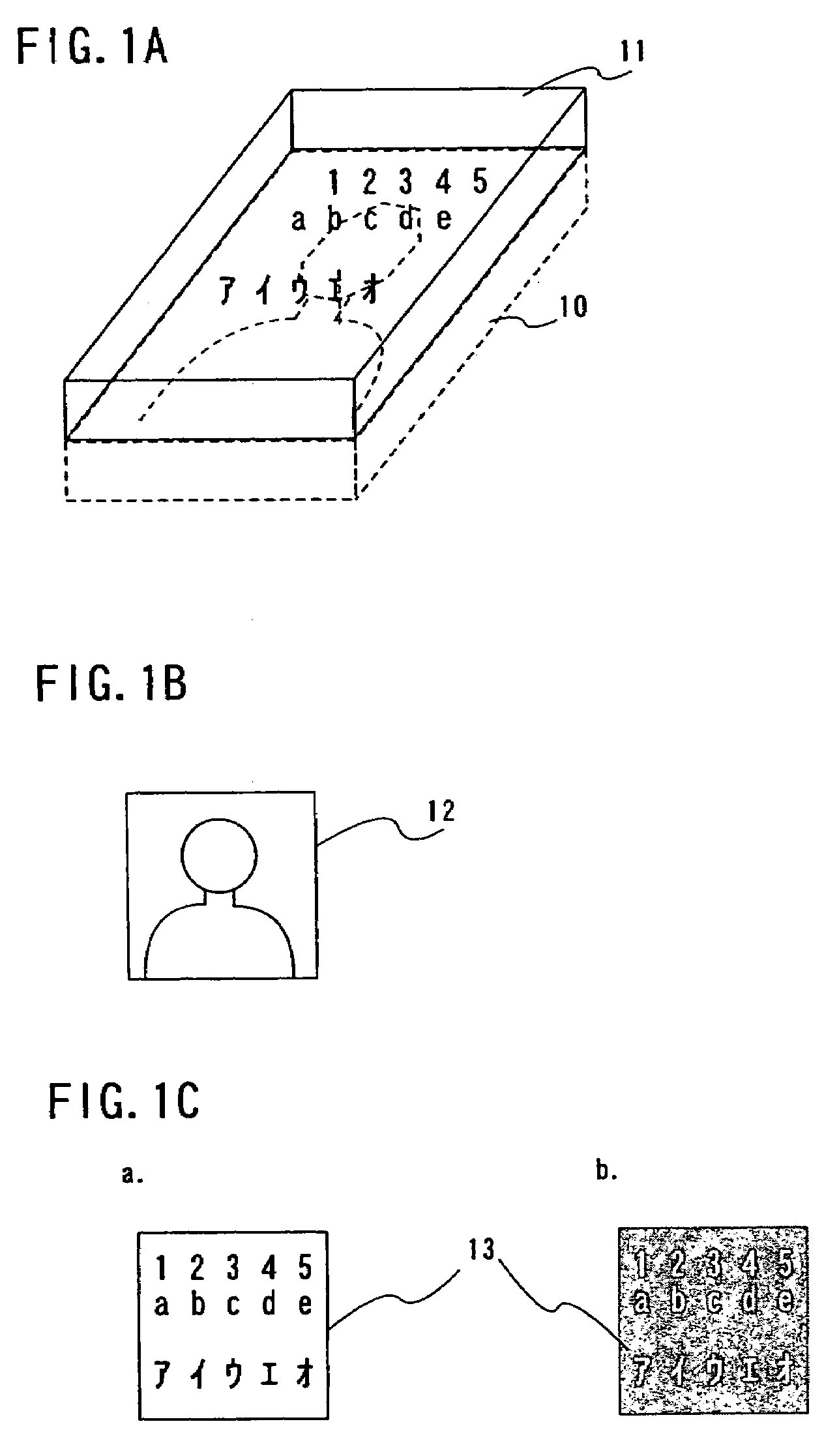
[0029]FIG. 1A shows a schematic view of a structure in which a first display area and a second display area are stacked together. A photograph is used for a first display area 10, and a dual emission light-emitting device is used for a second display area 11. The second display is shown by dotted lines and the first display is shown by a solid line.

[0030]FIG. 1B shows a state where the power of a second display area, namely a dual emission light-emitting device, is OFF. A dual emission light-emitting device is transparent when the power is OFF and display is not performed; then, the first display 12 can be recognized. Displaying means of the first display area is not limited to a photograph, and a liquid crystal display device, a light-emitting display device, electron paper, or the like may be used as described above.

[0031]FIG. 1C shows a state where the power of the second display area is ON, and display of a light-emitting device, that is second display 13, can be recognized. Whe...

embodiment mode 2

[0036]In this Embodiment Mode, a specific structure of a thin film integrated circuit device will be described by taking an IC card for instance.

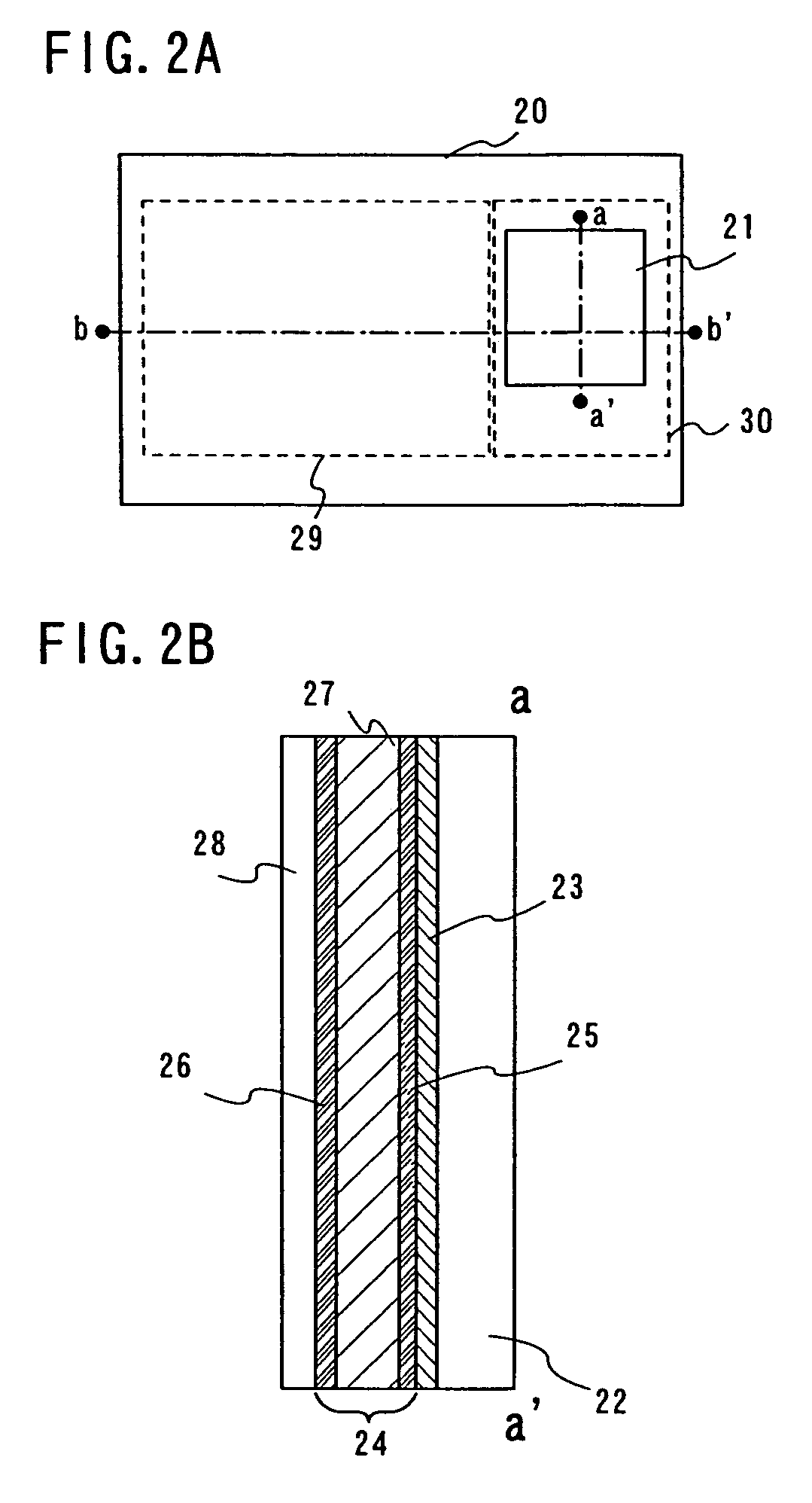
[0037]FIG. 2A shows an IC card 20 including a first display area using a photograph, a second display area 21 using a light-emitting device of a dual emission type (a dual emission EL display device), a thin film integrated circuit area 29, and a driver circuit 30 (display peripheral circuitry) for display.

[0038]FIG. 2B shows an enlarged view of a cross section taken along the line a-a′. A first display area 23 is provided over a substrate 22 of an IC card and a second display area 24 is provided in the cross sectional view. The first display area may use a photograph and an image is displayed (the first display). The first display area is adhered after the first display area is adhered on a substrate or an opening is formed in the substrate. A dual emission light-emitting device that is to be a second display area has a layer including an ...


PUM


Abstract

A device having an integrated circuit, especially an IC card, for reliably verifying a person's identity by display of PIN numbers or passwords with ingenuity. Portable electronic devices such as a PDA or a cellular phone, or other products can have plural displays in a display area (display part) provided in a limited area. A first display area and a second display area having transparency are stacked together in a thin film integrated circuit device of the present invention. The area of display can be reduced and display of more complicated PIN numbers or passwords is enabled by layering the display of the first display area and the display of the second display area.

Description

BACKGROUND OF THE INVENTION[0001]1. Field of the Invention[0002]The present invention relates to a thin film integrated circuit device including an integrated circuit such as a microprocessor (CPU), a memory. The present invention particularly relates to an IC card or a portable electronic device typified by a PDA and a cellular telephone.[0003]2. Description of the Related Art[0004]In recent years, as the field where an IC card is used is broaden, demand for an IC card having multifunctionality has been increasing. On the other hand, unauthorized use of IC cards increases and the countermeasure is urgently needed. An approach to the accurate personal-identification can be given as a countermeasure for the unauthorized use. As for a generally available IC card, the management using a personal identification number (PIN number) or a password, or printing a photograph of the face in a part of the card are given as methods for personal identification. Further, a method in which persona...

Claims


Application Information

Patent Timeline
Patent Type & Authority Patents(United States)
IPC IPC(8): G09G5/00G07F7/08G07F7/10H01L29/76H01L31/036H01L31/112
CPCG06K19/07703G07F7/086G07F7/1008G07F7/1025H01L27/3244H01L51/5234H01L2251/5323H10K59/12H10K50/828H10K2102/3031
Inventor YAMAZAKI, SHUNPEITACHIMURA, YUKOWATANABE, YASUKO
Owner SEMICON ENERGY LAB CO LTD
Learn More